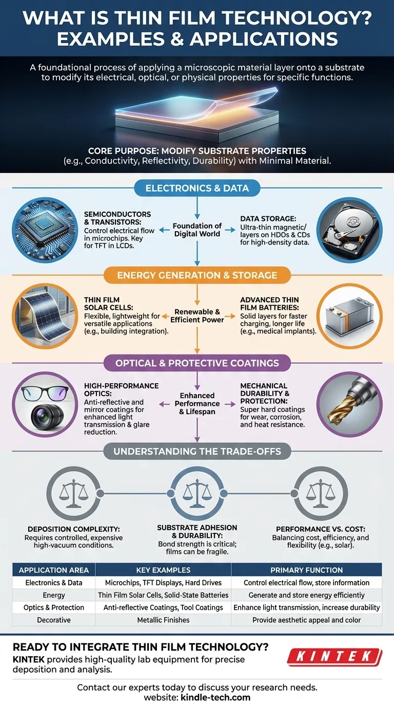
Thin film technology is a foundational process used to create everything from the screen you are reading this on to the advanced solar panels powering our world. Examples include the semiconductors in microchips, the anti-reflective coatings on eyeglasses, the light-emitting layers in OLED displays, the energy-producing layers in thin film solar cells, and the protective, wear-resistant coatings on industrial tools.
The core purpose of thin film technology is to apply a microscopic layer of material onto a surface, known as a substrate. This process fundamentally changes the substrate's properties—such as its electrical conductivity, optical reflectivity, or physical durability—to achieve a specific function using a minimal amount of material.
The Role of Thin Films in Electronics and Data
Modern electronics would not exist without the precise application of thin films. These layers, often just a few atoms thick, are the building blocks of the digital world.
Semiconductors and Transistors
Virtually all modern integrated circuits are built using thin film deposition. These layers create the pathways and gates that control the flow of electricity.
A key example is the Thin Film Transistor (TFT), which is essential for high-quality liquid crystal displays (LCDs). Each pixel in a display is controlled by its own TFT, enabling faster response times and greater energy efficiency.
Data Storage
Thin films are also central to how we store information. The surfaces of hard disk drives and CDs are coated with a precise, ultra-thin magnetic or optical layer.
It is this functional film that holds the data. The ability to deposit these layers with extreme uniformity is what allows for the incredible data density we rely on today.
Energy Generation and Storage
Thin film technology is driving significant advancements in the renewable energy sector by creating lighter, more flexible, and more efficient components.
Photovoltaic Solar Cells
Unlike traditional rigid silicon panels, thin film solar cells can be deposited on flexible substrates. This makes them significantly lighter and more versatile.
This flexibility allows for innovative applications, such as integrating solar-collecting films directly into building windows (photovoltaic glazing) or creating portable, roll-up solar chargers.
Advanced Batteries
Thin film batteries represent a major leap in energy storage. By replacing bulky liquid components with solid, ultra-thin layers, these batteries become more efficient, charge faster, and last longer.
This technology is critical for small-scale devices like medical implants and smart cards, as well as for large-scale green energy storage banks.
Optical and Protective Coatings
The first commercial uses of thin films were for optics, and this remains a primary application today, alongside creating highly durable protective surfaces.
High-Performance Optics
The simplest example of an optical thin film is a mirror, created by depositing a reflective metal like aluminum or silver onto glass. This process dates back over a century.
More advanced applications include the anti-reflective coatings on camera lenses and eyeglasses, which use multiple layers of thin films to minimize glare and maximize light transmission.
Mechanical Durability
In industrial settings, thin films are applied to cutting tools, engine parts, and other components to enhance their lifespan.
These super hard coatings provide exceptional resistance to wear, corrosion, heat, and oxidation, protecting the underlying material from failure in harsh operating conditions.
Decorative Finishes
On a simpler level, thin film deposition is used for purely cosmetic purposes, providing the metallic sheen on toys or adding durable, colored finishes to architectural fixtures and consumer products.
Understanding the Trade-offs
While incredibly powerful, thin film technology is not without its challenges. The benefits of a thin film are directly tied to the quality and complexity of its application.
Deposition Complexity
Applying a perfectly uniform, pure, and defect-free film requires highly controlled conditions, often involving high vacuums and expensive, specialized equipment. This complexity can be a significant barrier to manufacturing at scale.
Substrate Adhesion and Durability
A thin film is only as robust as its bond to the underlying substrate. If the film delaminates or peels away, its functional benefit is lost. The films themselves can also be physically fragile and susceptible to scratches or damage.
Performance vs. Cost
There is often a trade-off between different thin film characteristics. For instance, while some thin film solar cells are cheaper and more flexible than traditional silicon, they may offer lower energy conversion efficiency. Choosing the right deposition method and material is a balancing act between cost, performance, and durability.
How Thin Films Shape Different Industries
The right application of thin film technology depends entirely on the goal you want to achieve.
- If your primary focus is consumer electronics: Thin films are the non-negotiable foundation for creating high-resolution displays, powerful processors, and high-density data storage.
- If your primary focus is renewable energy: Thin film technology is key to developing lighter, more versatile solar panels and more efficient, faster-charging batteries.
- If your primary focus is industrial manufacturing: Thin films provide critical surface coatings that protect tools and components from wear, corrosion, and heat, dramatically extending their operational life.
Ultimately, thin film technology is one of the most important "invisible" innovations, enabling performance and functionality across nearly every modern industry.
Summary Table:
| Application Area | Key Examples | Primary Function |
|---|---|---|
| Electronics & Data | Microchips, TFT Displays, Hard Drives | Control electrical flow, store information |
| Energy | Thin Film Solar Cells, Solid-State Batteries | Generate and store energy efficiently |
| Optics & Protection | Anti-reflective Coatings, Wear-resistant Tool Coatings | Enhance light transmission, increase durability |
| Decorative | Metallic Finishes on Consumer Goods | Provide aesthetic appeal and color |
Ready to integrate thin film technology into your lab's workflow?
KINTEK specializes in providing the high-quality lab equipment and consumables necessary for precise thin film deposition and analysis. Whether you are developing next-generation semiconductors, advanced solar cells, or durable protective coatings, our solutions support the controlled conditions required for success.
Contact our experts today to discuss how we can help you achieve superior results in your thin film research and development.
Visual Guide
Related Products
- Vacuum Hot Press Furnace Machine for Lamination and Heating
- Electron Beam Evaporation Coating Oxygen-Free Copper Crucible and Evaporation Boat
- Thin-Layer Spectral Electrolysis Electrochemical Cell
- Lab Blown Film Extrusion Three Layer Co-Extrusion Film Blowing Machine
- Lab Plastic PVC Calender Stretch Film Casting Machine for Film Testing
People Also Ask
- What advantages does a vacuum hot press furnace provide for LSLBO ceramic electrolytes? Achieve 94% Relative Density
- What is the purpose of remelting heat treatment in a vacuum hot press for UHMWPE? Ensure Oxidative Stability
- What are the advantages of a vacuum hot press furnace for W-50%Cu? Achieve 99.6% Density at Lower Temperatures
- What role does mechanical pressure play during the vacuum diffusion bonding of tungsten and copper? Keys to Solid Bonding
- What is the application value of a vacuum hot press furnace? Unlock High-Density Complex Carbide Ceramics


