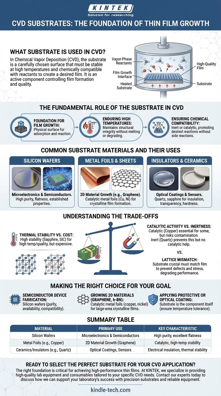
In Chemical Vapor Deposition (CVD), the substrate is not a single, universal material. Instead, it is a carefully chosen surface that must be stable at very high temperatures and chemically compatible with the gaseous reactants used to create the desired film. For example, materials like copper foil are commonly used as substrates to grow advanced materials like graphene.
The choice of a substrate is a critical design decision in any CVD process. It is not merely a passive holder but an active component whose thermal stability and chemical properties directly control the formation and quality of the final deposited film.
The Fundamental Role of the Substrate in CVD
To understand why certain materials are chosen, we must first understand the substrate's three primary functions within the CVD reactor.
The Foundation for Film Growth
The substrate provides the physical surface where vapor-phase chemical reactants adsorb and react to form a non-volatile solid film. The entire deposition process happens at the interface between the hot substrate and the surrounding gas.
Enduring High Temperatures
CVD is an elevated-temperature process, often conducted at or above 1000°C (1832°F). The substrate must maintain its structural and chemical integrity without melting, warping, or degrading under these extreme conditions.
Ensuring Chemical Compatibility
The substrate must be compatible with the precursor gases and the final film material. Ideally, it either remains inert or, in some cases, acts as a catalyst that actively promotes the desired chemical reaction while avoiding unwanted side reactions.
Common Substrate Materials and Their Uses
The specific substrate is chosen based on the material being deposited and the final application.
Silicon Wafers
For microelectronics and semiconductor fabrication, silicon wafers are the most common substrate. Their high purity, flatness, and well-understood properties make them the ideal foundation for building the integrated circuits found in virtually all modern electronics.
Metal Foils and Sheets
When growing advanced 2D materials like graphene, catalytic metal foils such as copper or copper-nickel alloys are used. These metals not only tolerate the high temperatures but also catalyze the breakdown of precursor gases (like methane) to form a high-quality, crystalline film on their surface.
Insulators and Ceramics
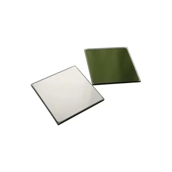
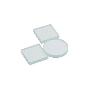
For applications requiring electrical insulation, optical transparency, or extreme hardness, substrates like quartz, sapphire, or various ceramics are employed. These are used for creating optical coatings, protective layers on sensor components, or films on other non-conductive devices.
Understanding the Trade-offs
Selecting a substrate involves balancing performance requirements with practical limitations.
Thermal Stability vs. Cost
Materials with exceptional thermal stability, like sapphire or silicon carbide, enable very high-temperature processes and superior film quality. However, they are significantly more expensive than materials like glass or standard silicon, which may limit the maximum process temperature.
Catalytic Activity vs. Inertness
A catalytic substrate like copper is essential for certain reactions but can also be a source of contamination if metal atoms diffuse into the growing film. An inert substrate like quartz prevents this but provides no catalytic assistance, which may result in slower growth rates or lower-quality films.
Lattice Mismatch
In advanced applications like epitaxy, the goal is to grow a perfectly ordered crystal film. The crystal structure of the substrate (its "lattice") must closely match that of the film to prevent defects. A significant lattice mismatch between the substrate and the film can introduce stress and imperfections, degrading performance.
Making the Right Choice for Your Goal
Your choice of substrate is determined entirely by the objective of your deposition process.
- If your primary focus is semiconductor device fabrication: Silicon wafers are the industry-standard choice due to their purity, availability, and established process compatibility.
- If your primary focus is growing 2D materials like graphene or h-BN: Catalytic metal foils like copper and nickel are required to facilitate the chemical reaction and produce large-area, crystalline films.
- If your primary focus is applying a protective or optical coating: The substrate will be the component itself (e.g., a tool bit, a lens), and the key is to ensure it can withstand the process temperature without damage.
Ultimately, selecting the correct substrate is the first critical step toward engineering a successful CVD process and achieving the desired film properties.
Summary Table:
| Substrate Material | Primary Use Case | Key Characteristic |
|---|---|---|
| Silicon Wafers | Microelectronics & Semiconductors | High purity, excellent flatness |
| Metal Foils (e.g., Copper) | 2D Material Growth (Graphene) | Catalytic, high-temperature stability |
| Ceramics/Insulators (e.g., Quartz) | Optical Coatings, Sensors | Electrical insulation, thermal stability |
Ready to select the perfect substrate for your CVD application? The right foundation is critical for achieving high-performance thin films. At KINTEK, we specialize in providing high-quality lab equipment and consumables tailored to your specific CVD needs. Whether you're working with semiconductor wafers, catalytic metal foils, or specialized ceramics, our expertise ensures your process runs efficiently and effectively. Contact our experts today to discuss how we can support your laboratory's success with precision substrates and reliable equipment.
Visual Guide
Related Products
- Conductive Carbon Cloth Carbon Paper Carbon Felt for Electrodes and Batteries
- Optical Window Glass Substrate Wafer Quartz Plate JGS1 JGS2 JGS3
- CVD Diamond for Thermal Management Applications
- Laboratory CVD Boron Doped Diamond Materials
- MgF2 Magnesium Fluoride Crystal Substrate Window for Optical Applications
People Also Ask
- What is a critical step when using carbon felt in an experiment? Ensure Complete Saturation for Maximum Efficiency
- What are the common applications for carbon cloth? Unlock Its Potential in Energy & Electrochemical Systems
- What are the examples of electrode materials? From Platinum to Graphite for Your Application
- How can the flexibility of carbon cloth be maintained over time? Preserve Mechanical Integrity with NAFION
- What is carbon cloth made of? Discover the Versatile High-Performance Fabric