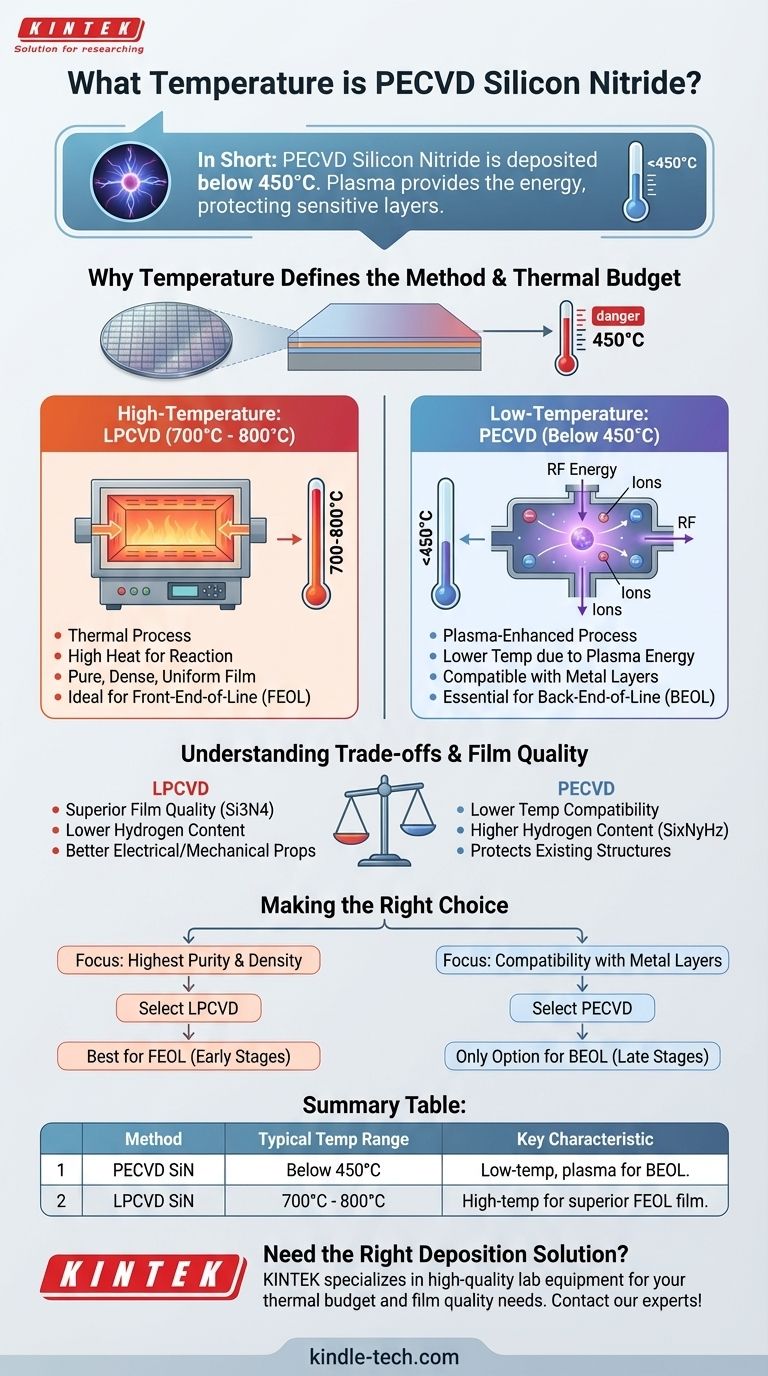
In short, PECVD silicon nitride is deposited at temperatures below 450°C. This relatively low temperature is the primary reason for its selection over alternative methods, which often require temperatures exceeding 700°C.
The critical takeaway is that PECVD uses plasma to provide the energy for the chemical reaction, allowing for a significantly lower deposition temperature. This makes it an essential tool for fabricating modern integrated circuits, where high temperatures could damage previously constructed layers.
Why Temperature Defines the Deposition Method
In semiconductor manufacturing, the "thermal budget" is a critical constraint. Every processing step adds heat, and the cumulative effect of this heat can alter or destroy the delicate structures already built on the wafer. Deposition methods are therefore often categorized by the temperature they require.
High-Temperature Deposition: LPCVD
Low-Pressure Chemical Vapor Deposition (LPCVD) is a thermal process. It relies on very high temperatures to give molecules the energy they need to react and form the desired film.
For silicon nitride, LPCVD typically operates at temperatures between 700°C and 800°C. This high heat produces a very pure, dense, and uniform film, making it ideal for certain applications.
Low-Temperature Deposition: PECVD
Plasma-Enhanced Chemical Vapor Deposition (PECVD) overcomes the need for extreme heat by using plasma. An RF or microwave energy source excites the precursor gases (like silane and ammonia), creating a highly reactive plasma.
This plasma provides the necessary reaction energy, allowing the deposition of silicon nitride at much lower temperatures—typically below 450°C. This fundamental difference is what gives PECVD its unique place in chip fabrication.
Understanding the Trade-offs: PECVD vs. LPCVD
Choosing between PECVD and LPCVD is not about which is "better," but which is appropriate for a specific stage of the manufacturing process. The decision is a clear engineering trade-off between film quality and thermal budget.
The Advantage of PECVD's Low Temperature
The primary benefit of PECVD is its compatibility with underlying device structures. By the time metal layers like aluminum are deposited, the wafer can no longer be exposed to temperatures above ~450°C without risking damage.
PECVD is therefore essential for depositing passivation or dielectric layers in the final stages of manufacturing, a process known as Back-End-of-Line (BEOL) fabrication.
The Film Quality of LPCVD
The trade-off for PECVD's lower temperature is often film quality. The chemical reaction SiHx + NH3 used in PECVD can result in significant amounts of hydrogen being incorporated into the final film, creating SixNyHz. This can affect the film's electrical properties and stability.
LPCVD, with its high thermal energy, typically produces a more stoichiometric and pure silicon nitride (Si3N4) film with lower hydrogen content and superior mechanical and electrical characteristics.
Making the Right Choice for Your Goal
Your choice of deposition method is dictated entirely by the fabrication stage and the requirements of the film.
- If your primary focus is the highest film purity and density: LPCVD is the superior choice, used when the thermal budget allows, such as in the early stages of fabrication (Front-End-of-Line).
- If your primary focus is compatibility with existing metal layers: PECVD is the only viable option, as its low temperature protects sensitive structures already on the device.
Ultimately, understanding the role of temperature is key to selecting the correct deposition tool for the job.
Summary Table:
| Deposition Method | Typical Temperature Range | Key Characteristic |
|---|---|---|
| PECVD Silicon Nitride | Below 450°C | Low-temperature, plasma-enhanced process for Back-End-of-Line (BEOL) fabrication. |
| LPCVD Silicon Nitride | 700°C - 800°C | High-temperature process for superior film quality in Front-End-of-Line (FEOL) stages. |
Need the Right Deposition Solution for Your Lab?
Choosing between PECVD and LPCVD is critical for your project's success. KINTEK specializes in providing high-quality lab equipment and consumables for all your semiconductor and materials science needs. Our experts can help you select the perfect tool to meet your thermal budget and film quality requirements.
Contact our team today to discuss how we can support your laboratory's goals!
Visual Guide
Related Products
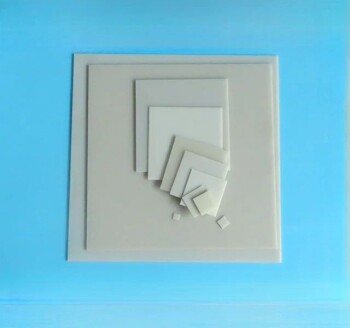
- Precision Machined Silicon Nitride (SiN) Ceramic Sheet for Engineering Advanced Fine Ceramics
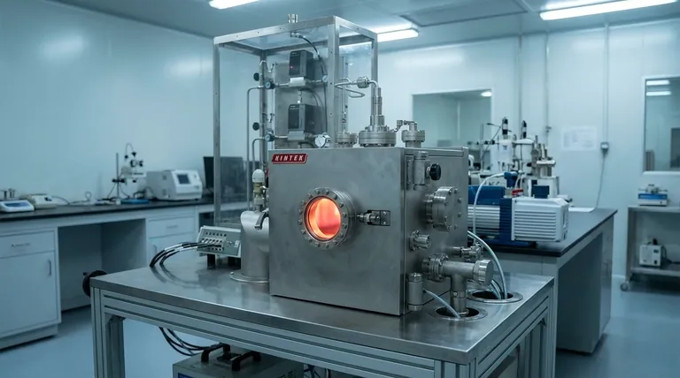
- Chemical Vapor Deposition CVD Equipment System Chamber Slide PECVD Tube Furnace with Liquid Gasifier PECVD Machine
- Inclined Rotary Plasma Enhanced Chemical Vapor Deposition PECVD Equipment Tube Furnace Machine
- Inclined Rotary Plasma Enhanced Chemical Vapor Deposition PECVD Equipment Tube Furnace Machine
- RF PECVD System Radio Frequency Plasma-Enhanced Chemical Vapor Deposition RF PECVD
People Also Ask
- What is the most commonly used in semiconductors? Discover Why Silicon Dominates Modern Electronics
- What are pure silicon sputtering targets? Precision Source for High-Performance Thin Films
- What is the sputtering target of gallium oxide? A Guide to High-Performance Ga₂O₃ Thin Films
- Which is the most preferred material for manufacturing of a semiconductor? Silicon's Dominance Explained
- What types of ceramics are used in sintering? Expert Guide to Advanced Materials and Forming