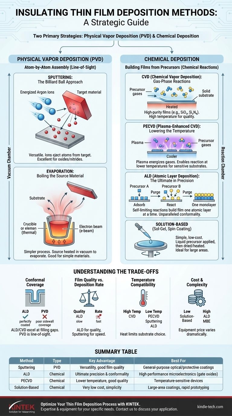
To deposit insulating thin films, engineers use a range of techniques, but they primarily fall into two categories: Physical Vapor Deposition (PVD) and Chemical Deposition. Common methods for insulators include sputtering and evaporation (from the PVD family), as well as Chemical Vapor Deposition (CVD), Plasma-Enhanced CVD (PECVD), and Atomic Layer Deposition (ALD) from the chemical family. The specific method chosen depends entirely on the required film quality, the material being deposited, and the project's budget.
The central challenge is not finding a method, but selecting the right one. The choice is a strategic trade-off between deposition speed, film quality, temperature sensitivity, and cost, with no single method being universally superior.
The Two Primary Deposition Strategies
Nearly all thin film deposition techniques can be classified as either physical or chemical. Understanding this distinction is the first step in choosing the correct process for your insulating layer.
Physical Vapor Deposition (PVD): Atom-by-Atom Assembly
PVD methods involve physically transforming a solid source material into a vapor within a vacuum chamber. This vapor then travels and condenses onto the target substrate, forming the thin film.
These methods are "line-of-sight," meaning the atoms travel in a straight line from the source to the substrate.
Sputtering: The Billiard Ball Approach
Sputtering is a highly versatile PVD technique. It uses an energized gas (typically argon) to create a plasma, whose ions bombard a solid "target" of the desired insulating material.
This bombardment ejects atoms from the target like billiard balls, which then deposit onto the substrate. Sputtering is excellent for depositing a wide range of materials, including oxides and nitrides, which are common insulators.
Thermal & E-Beam Evaporation: Boiling the Source Material
Evaporation is a simpler PVD process where the source material is heated in a vacuum until it evaporates or sublimes. The resulting vapor coats the substrate.
Heating can be done with a resistive element (thermal evaporation) or a high-energy electron beam (e-beam evaporation). While effective for simple materials, it can be difficult to control the composition of complex insulators.
Chemical Deposition: Building Films from Precursors
Instead of using a solid source, chemical deposition methods introduce precursor gases or liquids into a reaction chamber. Chemical reactions then occur on the substrate's surface, building the film molecule by molecule.
Chemical Vapor Deposition (CVD): Gas-Phase Reactions
CVD is a workhorse of the semiconductor industry for creating high-purity insulating films like silicon dioxide (SiO₂) and silicon nitride (Si₃N₄).
In this process, precursor gases flow over a heated substrate, triggering a chemical reaction that leaves a solid film behind. The high temperatures required often lead to excellent film quality.
Plasma-Enhanced CVD (PECVD): Lowering the Temperature
PECVD is a variation of CVD that uses a plasma to energize the precursor gases. This allows the chemical reaction to occur at much lower temperatures.
This is critical when depositing films on substrates that cannot withstand the high heat of traditional CVD, such as plastics or fully processed semiconductor wafers.
Atomic Layer Deposition (ALD): The Ultimate in Precision
ALD offers the highest level of control possible. It builds the film one single atomic layer at a time through a sequence of self-limiting chemical reactions.
This method provides unparalleled uniformity and the ability to perfectly coat highly complex, three-dimensional structures. However, it is significantly slower and more expensive than other techniques.
Solution-Based Methods (Sol-Gel, Spin Coating)
Simpler chemical methods like sol-gel, dip coating, and spin coating involve applying a liquid chemical precursor to the substrate. The film is then formed by spinning the substrate to create a uniform layer and then drying or heating it.
These methods are low-cost and ideal for large-area applications or rapid prototyping where ultimate precision is not the primary concern.
Understanding the Trade-offs
Choosing a deposition method requires balancing competing factors. What makes one process ideal for a specific application makes it unsuitable for another.
Conformal Coverage: Filling the Gaps
Conformal coverage refers to a film's ability to coat complex, non-flat topographies with a uniform thickness.
Chemical methods like CVD and especially ALD excel here because the precursor gases can reach every nook and cranny. PVD methods, being line-of-sight, struggle to coat sidewalls and trenches effectively.
Film Quality vs. Deposition Rate
There is almost always a trade-off between quality and speed. ALD produces nearly perfect films but is extremely slow.
Sputtering and evaporation offer much higher deposition rates but may result in films with lower purity or more structural defects compared to high-temperature CVD.
Temperature and Substrate Compatibility
The heat required for a deposition process can limit your choice of substrate.
High-temperature CVD produces excellent films but can damage sensitive electronic components or polymer substrates. In these cases, lower-temperature processes like PECVD, sputtering, or ALD are necessary.
Cost and Complexity
The equipment for deposition varies dramatically in price. Sol-gel or spin coating can be done with simple lab equipment.
In contrast, systems for ALD or Molecular Beam Epitaxy (MBE) are highly complex and represent a significant capital investment, reserved for the most demanding applications.
Selecting the Right Method for Your Insulator
Your choice should be guided by your end goal. Match the process capabilities to your project's specific technical and budget requirements.
- If your primary focus is high-performance microelectronics: Use ALD for perfect, conformal gate oxides or PECVD for balanced performance on temperature-sensitive devices.
- If your primary focus is general-purpose optical coatings or protective layers: Use sputtering for its versatility, good film quality, and reasonable deposition speed.
- If your primary focus is large-area coatings or rapid prototyping: Use solution-based methods like spin coating or sol-gel for their extremely low cost and simplicity.
Ultimately, selecting the correct deposition method is a strategic engineering decision based on a clear understanding of your project's unique constraints and goals.
Summary Table:
| Method | Type | Key Advantage | Best For |
|---|---|---|---|
| Sputtering | PVD | Versatility, good film quality | General-purpose optical/protective coatings |
| ALD (Atomic Layer Deposition) | Chemical | Ultimate precision & conformality | High-performance microelectronics (gate oxides) |
| PECVD (Plasma-Enhanced CVD) | Chemical | Lower temperature, good quality | Temperature-sensitive devices (e.g., on processed wafers) |
| Solution-Based (Spin Coating) | Chemical | Very low cost, simplicity | Large-area coatings, rapid prototyping |
Optimize Your Thin Film Deposition Process with KINTEK
Choosing the right deposition method is critical to the success of your project. Whether you require the ultimate precision of ALD for advanced semiconductor applications, the versatility of sputtering for R&D, or the cost-effectiveness of solution-based methods, KINTEK has the expertise and equipment to meet your laboratory's specific needs.
Our specialists can help you navigate the trade-offs between film quality, deposition rate, and cost to identify the perfect solution for your insulating thin film requirements.
Contact our experts today to discuss your application and discover how KINTEK's lab equipment and consumables can enhance your research and development.
Visual Guide
Related Products
- Chemical Vapor Deposition CVD Equipment System Chamber Slide PECVD Tube Furnace with Liquid Gasifier PECVD Machine
- Customer Made Versatile CVD Tube Furnace Chemical Vapor Deposition Chamber System Equipment
- Split Chamber CVD Tube Furnace with Vacuum Station Chemical Vapor Deposition System Equipment Machine
- Multi Heating Zones CVD Tube Furnace Machine Chemical Vapor Deposition Chamber System Equipment
- RF PECVD System Radio Frequency Plasma-Enhanced Chemical Vapor Deposition RF PECVD
People Also Ask
- What is plasma enhanced chemical vapor deposition PECVD equipment? A Guide to Low-Temperature Thin Film Deposition
- What happens during deposition chemistry? Building Thin Films from Gaseous Precursors
- What are the advantages of chemical vapor deposition? Achieve Superior Thin Films for Your Lab
- How expensive is chemical vapor deposition? Understanding the True Cost of High-Performance Coating
- Why is Chemical Vapor Deposition (CVD) equipment uniquely suited for constructing hierarchical superhydrophobic structures?


