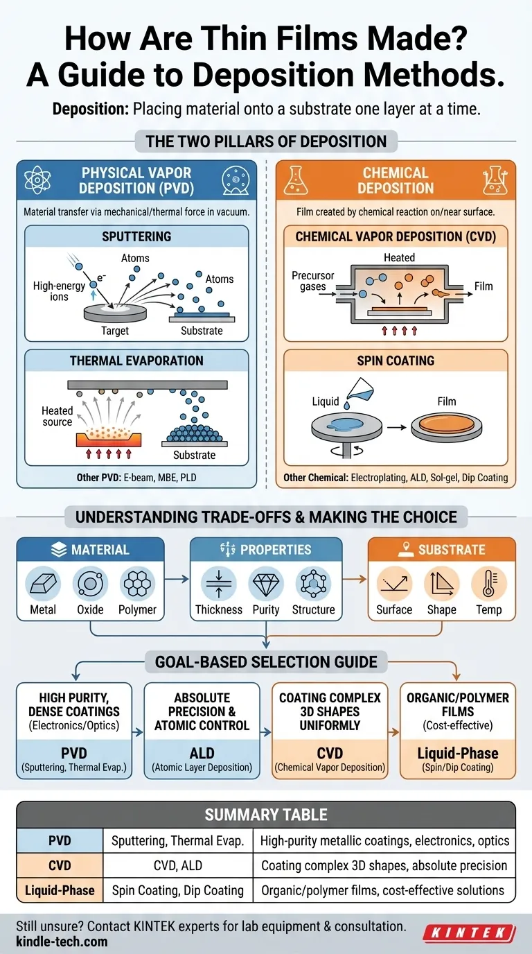
To make a thin film, you must use a deposition method, a process that places material onto a substrate one layer at a time. The most common and foundational techniques include physical methods like sputtering and thermal evaporation, as well as chemical methods like chemical vapor deposition (CVD) and spin coating. These processes allow for precise control over the film's thickness, composition, and final properties.
The core principle to understand is that all thin film creation methods fall into two major categories: Physical Deposition and Chemical Deposition. The ideal choice between them is not about which is "best" overall, but which is best suited for the specific material, the substrate it's being applied to, and the desired outcome of the film.
The Two Pillars of Thin Film Deposition
At the highest level, creating a thin film involves moving material from a source to a surface (the substrate). The fundamental difference lies in how that material is moved and deposited.
Understanding Physical Vapor Deposition (PVD)
Physical Vapor Deposition encompasses a family of techniques that use mechanical, thermal, or electrical force to transfer material in a vacuum environment. The material being deposited starts in a solid form, is converted into a vapor, and then condenses on the substrate as a thin film.
Sputtering is a cornerstone of PVD. In this process, a solid "target" of the desired material is bombarded with high-energy ions, which physically knock atoms loose. These ejected atoms then travel and deposit onto the substrate.
Thermal Evaporation is another key PVD technique. It involves heating a source material in a high vacuum until it vaporizes. This vapor then travels through the vacuum chamber and condenses on a cooler substrate, forming the film.
Other important PVD methods include electron beam evaporation, molecular beam epitaxy (MBE), and pulsed laser deposition (PLD).
Understanding Chemical Deposition Methods
Chemical methods rely on a chemical reaction to create the film. Precursor materials, often in gas or liquid form, react on or near the substrate surface, leaving behind the desired solid film as a byproduct.
Chemical Vapor Deposition (CVD) is the most prominent example. In CVD, precursor gases are introduced into a reaction chamber where they decompose and react on a heated substrate to form the film.
Spin Coating is a widely used liquid-phase technique, particularly for polymers. A solution containing the desired material is applied to the center of a substrate, which is then spun at high speed to spread the liquid into a uniform thin film as the solvent evaporates.
Other common chemical methods include electroplating, atomic layer deposition (ALD), sol-gel, and dip coating.
Understanding the Trade-offs
Choosing the right deposition method is a critical decision determined by technical requirements and practical constraints. There is no single solution for all applications.
The Role of the Material
The material you intend to deposit—be it a metal, oxide, polymer, or compound—is a primary decision driver. Many high-purity metals and compounds are best handled with PVD methods like sputtering, whereas polymers are almost always applied using liquid-phase methods like spin coating.
Desired Film Properties
The required thickness, purity, and structure of the final film dictate the method. For creating exceptionally thin, uniform, and precise layers down to a single atom, Atomic Layer Deposition (ALD) is unparalleled. For creating thicker, robust metallic coatings, sputtering is often more efficient.
The Substrate Matters
The substrate's surface, shape, and temperature tolerance are crucial. CVD, for example, is excellent for coating complex, non-flat surfaces uniformly. However, the high temperatures required for some CVD processes can damage sensitive substrates, making a lower-temperature PVD process a better choice.
Making the Right Choice for Your Goal
Your application's primary goal will guide you to the most appropriate category of deposition methods.
- If your primary focus is high-purity, dense coatings for electronics or optics: PVD methods like sputtering and thermal evaporation offer excellent control and material quality.
- If your primary focus is absolute precision and atomic-level thickness control: Atomic Layer Deposition (ALD) is the superior chemical method for this task.
- If your primary focus is coating complex 3D shapes uniformly: Chemical Vapor Deposition (CVD) provides excellent conformity over intricate surfaces.
- If your primary focus is creating organic or polymer films cost-effectively: Liquid-phase methods like spin coating, dip coating, or drop casting are simple and highly effective.
Ultimately, selecting the correct method requires aligning the strengths of each technique with the specific demands of your material and application.
Summary Table:
| Method Category | Key Techniques | Best For |
|---|---|---|
| Physical Vapor Deposition (PVD) | Sputtering, Thermal Evaporation | High-purity metallic coatings, electronics, optics |
| Chemical Vapor Deposition (CVD) | CVD, Atomic Layer Deposition (ALD) | Coating complex 3D shapes, absolute precision |
| Liquid-Phase Deposition | Spin Coating, Dip Coating | Organic/polymer films, cost-effective solutions |
Still Unsure Which Thin Film Deposition Method is Right for Your Project?
Choosing between PVD, CVD, and other techniques is critical for achieving the desired film properties, from thickness and purity to uniformity. The experts at KINTEK specialize in lab equipment and consumables for all deposition methods, serving the precise needs of research and industrial laboratories.
We can help you navigate the trade-offs to select the ideal equipment for your specific material, substrate, and application goals. Contact us today for a personalized consultation to ensure your thin film success.
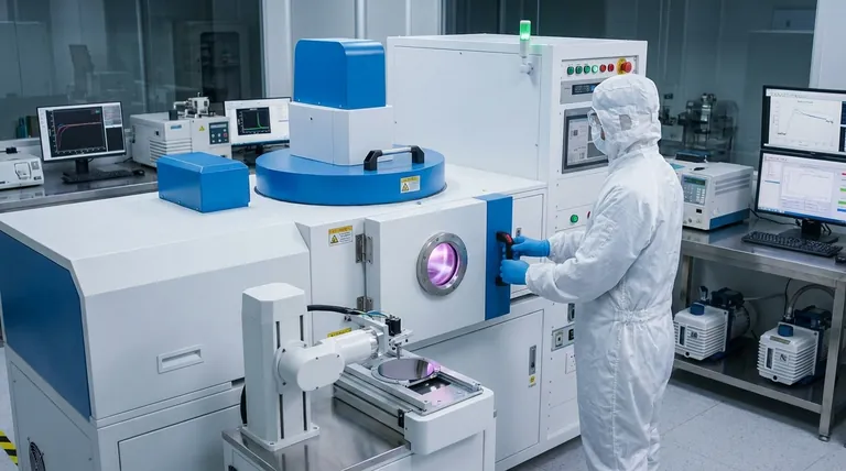
Visual Guide
Related Products
- Aluminized Ceramic Evaporation Boat for Thin Film Deposition
- Tungsten Evaporation Boat for Thin Film Deposition
- Electron Beam Evaporation Coating Oxygen-Free Copper Crucible and Evaporation Boat
- Molybdenum Tungsten Tantalum Evaporation Boat for High Temperature Applications
- HFCVD Machine System Equipment for Drawing Die Nano-Diamond Coating
People Also Ask
- What are thin films deposited by evaporation? A Guide to High-Purity Coating
- Why is an alumina boat and Ti3AlC2 powder bed necessary for Ti2AlC sintering? Protect MAX Phase Purity
- What is the source of evaporation for thin film? Choosing Between Thermal and E-Beam Methods
- Why are high-purity ceramic boats used for lignin activation? Ensure Purity & Thermal Stability
- What is the widely used boat made of in thermal evaporation? Choosing the Right Material for High-Purity Deposition


