At its core, samples for Scanning Electron Microscopy (SEM) are coated with carbon to make non-conductive specimens electrically conductive. This prevents a disruptive build-up of electron charge on the sample surface, which would otherwise distort the image. Carbon is chosen specifically when the goal includes elemental analysis, as its properties do not interfere with identifying the composition of the underlying sample.
The decision to use carbon coating is not arbitrary; it is a strategic choice. While all conductive coatings aim to prevent charging, carbon is uniquely suited for applications requiring elemental analysis (EDS/EDX) because its low atomic number does not obscure the characteristic X-ray signals from the specimen itself.
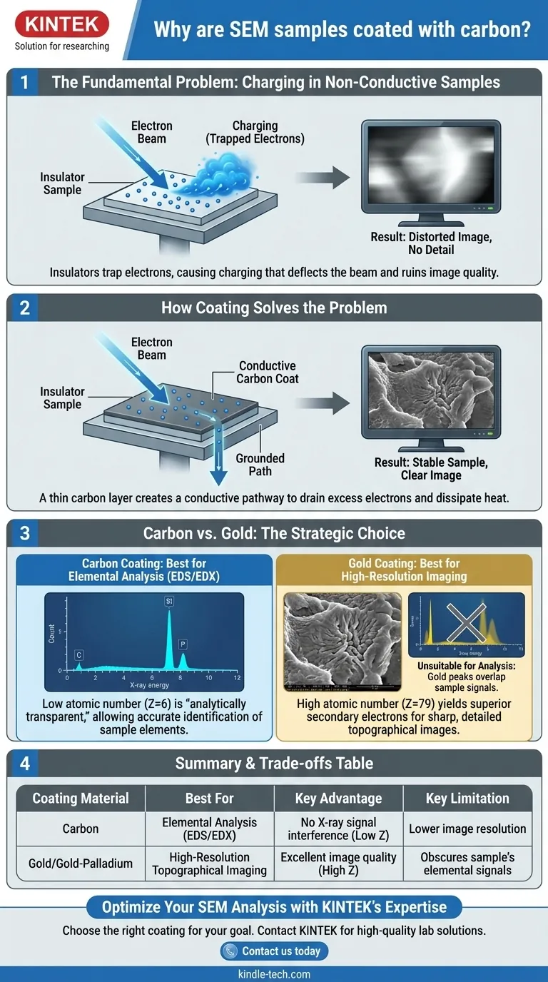
The Fundamental Problem: Charging in Non-Conductive Samples
What is Sample Charging?
A Scanning Electron Microscope works by bombarding a specimen with a focused beam of high-energy electrons.
When the specimen is electrically conductive (like a metal), these incoming electrons have a path to flow away to the grounded sample holder.
However, if the specimen is an insulator (like a polymer, ceramic, or biological tissue), the electrons accumulate on the surface. This phenomenon is known as charging.
The Impact of Charging
This trapped negative charge deflects the incoming electron beam and distorts the signals used to create an image.
The result is severe image artifacts, such as abnormally bright patches, shifting or drifting of the image, and a complete loss of surface detail. In short, charging makes it impossible to acquire a clear and stable image.
How Coating Solves the Problem
Creating a Conductive Pathway
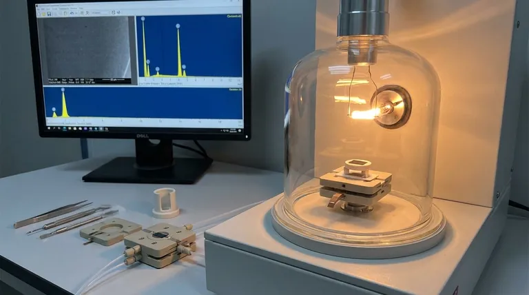
To solve the charging issue, a very thin layer of a conductive material is deposited onto the sample's surface. This is most often done via sputter coating or carbon evaporation.
This conductive film is connected to the metal SEM stub (sample holder), which is grounded. It provides an effective pathway for excess electrons to drain away, neutralizing the charge build-up and stabilizing the specimen under the beam.
Additional Benefits of Coating
Beyond preventing charging, a conductive coat improves SEM performance in several ways.
It increases thermal conduction, which helps dissipate heat from the electron beam and protects delicate samples from damage. It also enhances the emission of secondary electrons, which are the primary signal used for creating high-resolution images of surface topography.
Carbon vs. Gold: Choosing the Right Coat
The two most common coating materials are carbon and gold (or a gold-palladium alloy). The choice between them depends entirely on your analytical goal.
The Case for Carbon: Elemental Analysis (EDS/EDX)
The primary reason to choose carbon is for Energy-Dispersive X-ray Spectroscopy (EDS or EDX). This technique analyzes the X-rays emitted from the sample to determine its elemental composition.
Carbon has a very low atomic number (Z=6). Its characteristic X-ray peak is low in energy and does not overlap with the peaks of most other elements. This makes carbon an "analytically transparent" coating that allows for accurate elemental identification of the underlying specimen.
The Case for Gold: High-Resolution Imaging
Gold has a high atomic number (Z=79) and is an extremely efficient emitter of secondary electrons.
This high signal yield results in images with an excellent signal-to-noise ratio, producing exceptionally sharp, crisp, and high-resolution views of the sample's surface topography. If your only goal is to see the surface structure in the highest possible detail, gold is the superior choice.
Understanding the Trade-offs
Carbon: Best for Analysis, Good for Imaging
While carbon provides good conductivity, its secondary electron yield is lower than gold's. This means the resulting image might appear slightly "noisier" or less sharp compared to a gold-coated sample. It is a functional compromise to enable chemical analysis.
Gold: Superior for Imaging, Unsuitable for Analysis
The high atomic number of gold that makes it great for imaging is precisely what makes it terrible for EDS. Gold produces a complex series of strong X-ray peaks that can overlap with and completely obscure the signals from elements within your sample (e.g., phosphorus, sulfur, silicon), making accurate elemental analysis impossible.
Coating Thickness and Quality
Regardless of the material, the coating must be thin (typically 5-20 nanometers) and uniform. A coat that is too thick will obscure the fine surface details you want to see, while a non-uniform coat will fail to prevent charging across the entire surface.
Making the Right Choice for Your Goal
The material you use to coat your sample is a critical decision that dictates what you can achieve in the SEM.
- If your primary focus is elemental composition (EDS/EDX): You must use carbon coating to ensure the analytical signals from your sample are not obscured.
- If your primary focus is high-resolution surface imaging (topography): Use a metal coating like gold or gold-palladium for the best possible image quality and signal-to-noise ratio.
- If you need to analyze an extremely beam-sensitive sample: Carbon coating can also be preferable as it helps dissipate heat without adding the heavy metal artifacts of gold.
Ultimately, your choice of coating directly enables or disables specific analytical capabilities for your experiment.
Summary Table:
| Coating Material | Best For | Key Advantage | Key Limitation |
|---|---|---|---|
| Carbon | Elemental Analysis (EDS/EDX) | Low atomic number avoids X-ray signal interference | Lower secondary electron yield for imaging |
| Gold/Gold-Palladium | High-Resolution Topographical Imaging | High secondary electron yield for sharp, detailed images | Strong X-ray peaks obscure sample's elemental signals |
Optimize Your SEM Analysis with KINTEK's Expertise
Choosing the right coating is critical for successful SEM results. Whether your priority is flawless elemental analysis with carbon or ultra-high-resolution imaging with gold, KINTEK has the solution. We specialize in providing high-quality lab equipment and consumables tailored to your laboratory's specific needs.
Contact us today using the form below to discuss how our products can enhance your SEM workflow and deliver reliable, high-quality data. Let KINTEK be your partner in precision.
Visual Guide
Related Products
- Conductive Carbon Cloth Carbon Paper Carbon Felt for Electrodes and Batteries
- Professional Cutting Tools for Carbon Paper Cloth Diaphragm Copper Aluminum Foil and More
- Electron Beam Evaporation Coating Oxygen-Free Copper Crucible and Evaporation Boat
- Hydrophilic Carbon Paper TGPH060 for Battery Lab Applications
- Custom CVD Diamond Coating for Lab Applications
People Also Ask
- How can the flexibility of carbon cloth be maintained over time? Preserve Mechanical Integrity with NAFION
- What are the electrode materials? A Guide to Choosing the Right Conductor for Your Application
- How should carbon materials be cleaned before use? Ensure Peak Performance with Proper Prep
- What are the material properties of carbon cloth? Harness Strength, Conductivity & Flexibility
- What are the common applications for carbon cloth? Unlock Its Potential in Energy & Electrochemical Systems