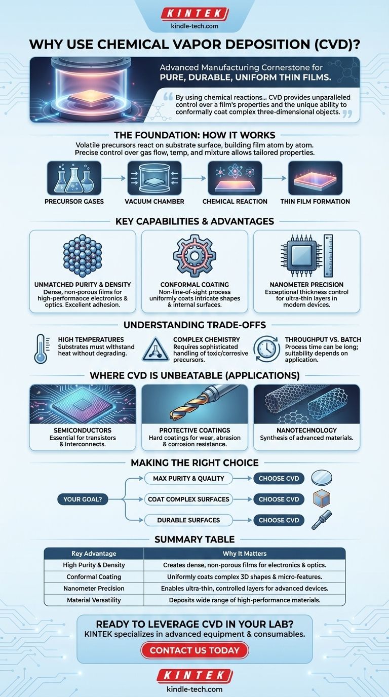
In advanced manufacturing and materials science, chemical vapor deposition (CVD) is a cornerstone technology used for its unique ability to grow exceptionally pure, durable, and uniform thin films. The process relies on controlled chemical reactions in a vacuum, allowing it to deposit high-performance coatings onto a vast range of materials, including those with complex and intricate surfaces that other methods cannot uniformly cover.
The fundamental reason to use chemical vapor deposition is not just its versatility, but its core mechanism. By using chemical reactions instead of physical transfer, CVD provides unparalleled control over a film's properties and the unique ability to conformally coat complex three-dimensional objects.
The Foundation: How Chemical Reactions Drive Deposition
What is Chemical Vapor Deposition?
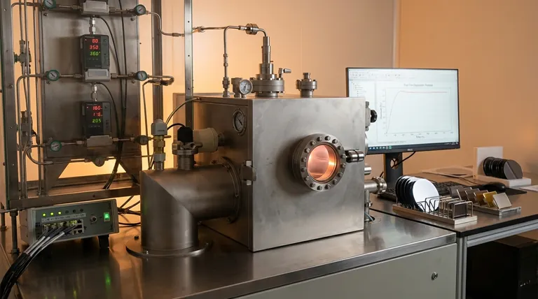
Chemical vapor deposition is a process where a substrate (the object to be coated) is placed in a vacuum chamber and exposed to volatile precursor gases.
These gases react or decompose on the substrate's surface, leaving behind a solid material in the form of a thin film. This chemical transformation is the defining characteristic of CVD.
The Power of Chemical Precursors
The "vapor" in CVD refers to the precursor chemicals, which are specifically chosen to yield the desired film material.
By precisely controlling the mixture, flow rate, and temperature of these gases, engineers can tailor the final coating's properties. This allows for the creation of films optimized for high purity, corrosion resistance, electrical conductivity, or extreme durability.
Key Capabilities That Define CVD
Unmatched Purity and Density
Because CVD builds a film atom by atom through chemical reactions, it can produce materials with extremely high purity and structural integrity.
This results in dense, non-porous films with excellent adhesion, which is critical for high-performance applications in electronics and optics.
Conformal Coating for Complex Geometries
Unlike line-of-sight methods like physical vapor deposition (PVD), the precursor gases in a CVD process can flow around and into complex shapes.
This non-line-of-sight nature ensures that even intricate components, internal surfaces, and micro-scale features receive a completely uniform, or conformal, coating.
Precision Control Down to the Nanometer
The process offers exceptional control over the thickness of the deposited film, making it possible to create ultra-thin layers with nanometer-scale precision.
This level of control is essential for modern electronics, where the performance of a semiconductor device is determined by the thickness and quality of its multiple stacked layers.
Understanding the Trade-offs
High Processing Temperatures
Many CVD processes require high temperatures to initiate the necessary chemical reactions on the substrate's surface.
This can be a limitation, as the substrate material must be able to withstand the heat without melting, warping, or degrading. This factor often dictates which materials are suitable for a specific CVD process.
Precursor Chemistry and Safety
The gases used as precursors in CVD can be toxic, flammable, or corrosive, requiring sophisticated handling, delivery, and exhaust management systems.
This adds a layer of operational complexity and cost compared to simpler coating methods.
Throughput vs. Batch Size
While CVD has a relatively high deposition rate, the overall process time can be long due to chamber heating, vacuum pumping, and cooling cycles.
It is often a batch process, meaning its suitability for very high-volume, continuous manufacturing depends heavily on the specific application and equipment.
Where CVD is the Unbeatable Choice
Semiconductor and Electronics Manufacturing
CVD is indispensable for building the microscopic integrated circuits on silicon wafers. It is used to deposit the insulating, conducting, and semiconducting layers that form transistors and interconnects.
Protective Coatings for Tools and Components
Hard, durable coatings of materials like titanium nitride or diamond-like carbon are applied to cutting tools, bearings, and engine parts using CVD. These coatings dramatically increase resistance to wear, abrasion, and corrosion.
Advanced Materials and Nanotechnology
CVD is a primary method for synthesizing advanced materials. It is used to grow carbon nanotubes, graphene, and various nanowires, which are foundational materials for next-generation technologies.
Making the Right Choice for Your Application
Choosing a deposition method requires understanding your primary goal.
- If your primary focus is maximum purity and film quality: CVD is the leading choice for creating the dense, defect-free semiconductor and optical layers required for high-performance devices.
- If your primary focus is coating complex, non-flat surfaces: CVD's non-line-of-sight nature ensures a uniform, conformal coating that physical methods cannot achieve.
- If your primary focus is creating durable, high-performance surfaces: CVD delivers robust coatings that resist wear, corrosion, and extreme temperatures, making it ideal for industrial tools and aerospace components.
Ultimately, chemical vapor deposition is the enabling technology that translates the blueprint of chemistry into the high-performance materials that define modern engineering.
Summary Table:
| Key Advantage | Why It Matters |
|---|---|
| High Purity & Density | Creates dense, non-porous films essential for high-performance electronics and optics. |
| Conformal Coating | Uniformly coats complex 3D shapes, including internal surfaces and micro-features. |
| Nanometer Precision | Enables ultra-thin, precisely controlled layers for advanced semiconductor devices. |
| Material Versatility | Deposits a wide range of high-performance materials like diamond-like carbon and graphene. |
Ready to leverage the power of Chemical Vapor Deposition in your lab?
KINTEK specializes in providing advanced lab equipment and consumables for materials science and manufacturing. Whether you are developing next-generation semiconductors, creating durable protective coatings, or synthesizing advanced nanomaterials, our expertise can help you achieve superior results.
Contact us today to discuss how our solutions can meet your specific laboratory needs and drive your innovations forward.
Visual Guide
Related Products
- Chemical Vapor Deposition CVD Equipment System Chamber Slide PECVD Tube Furnace with Liquid Gasifier PECVD Machine
- RF PECVD System Radio Frequency Plasma-Enhanced Chemical Vapor Deposition RF PECVD
- Microwave Plasma Chemical Vapor Deposition MPCVD Machine System Reactor for Lab and Diamond Growth
- Customer Made Versatile CVD Tube Furnace Chemical Vapor Deposition Chamber System Equipment
- 915MHz MPCVD Diamond Machine Microwave Plasma Chemical Vapor Deposition System Reactor
People Also Ask
- What are the core advantages of PE-CVD in OLED encapsulation? Protect Sensitive Layers with Low-Temp Film Deposition
- How expensive is chemical vapor deposition? Understanding the True Cost of High-Performance Coating
- What are the advantages of chemical vapor deposition? Achieve Superior Thin Films for Your Lab
- What is plasma enhanced chemical vapor deposition PECVD equipment? A Guide to Low-Temperature Thin Film Deposition
- What is the chemical vapor deposition growth process? Build Superior Thin Films from the Atom Up


