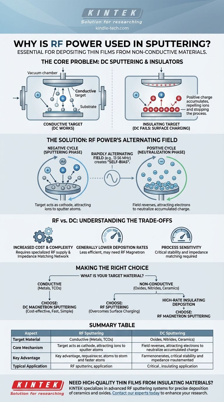
At its core, RF power is used in sputtering to deposit thin films from non-conductive materials. A standard DC (Direct Current) power supply is ineffective for these insulating or dielectric targets, such as ceramics and oxides. RF (Radio Frequency) power overcomes this fundamental limitation by using an alternating electric field, making it an essential technology in the semiconductor and advanced materials industries.
The central problem with sputtering an insulator is "positive charge buildup." A standard DC process bombards the target with positive ions, but an insulator cannot dissipate this charge. RF power solves this by rapidly alternating the electric field, using a brief positive cycle to attract electrons and neutralize this charge, allowing the sputtering process to continue.
The Fundamental Challenge: Sputtering Insulators
To understand why RF is necessary, we must first understand why the simpler, more common DC sputtering method fails when used with non-conductive materials.
Why Standard DC Sputtering Fails
In DC sputtering, a high negative voltage is applied to a conductive target material. This attracts positive ions (typically from an inert gas like Argon) from the plasma.
These ions strike the target with high energy, dislodging or "sputtering" atoms, which then deposit onto a substrate.
When this same process is applied to an insulating target, the positive ions accumulate on the surface. Since the material is an insulator, this positive charge has nowhere to go. This effect, known as surface charging, repels any further incoming positive ions, effectively stopping the sputtering process almost immediately.
How RF Power Solves the Sputtering Puzzle
RF sputtering uses a high-frequency alternating current (AC) power source, typically at 13.56 MHz, instead of a constant DC voltage. This alternating field is the key to overcoming the surface charging problem.
The Negative Cycle: The "Sputtering" Phase
During the negative portion of the RF cycle, the target acts just like a cathode in a DC system. It is negatively charged and attracts the positive argon ions from the plasma.
This ion bombardment successfully sputters atoms from the target material, just as intended. However, this phase also causes the problematic positive charge to begin building up on the insulating surface.
The Positive Cycle: The "Neutralization" Phase
Before the positive charge can build up enough to stop the process, the RF field reverses. During the brief positive cycle, the target surface becomes positively charged.
This immediately attracts a flood of highly mobile electrons from the plasma. These electrons effectively neutralize the positive charge that accumulated during the negative cycle, essentially "resetting" the target surface for the next sputtering phase.
Creating a "Self-Bias"
Because electrons are thousands of times lighter and more mobile than the heavy argon ions, they can respond to the changing field much faster. This results in the target developing a net negative charge over time, known as a self-bias. This ensures that ion bombardment remains efficient while still allowing for the critical charge neutralization step.
Understanding the Trade-offs of RF Sputtering
While essential for insulators, the RF approach is not a universal replacement for DC sputtering. It comes with its own set of technical and economic considerations.
Increased Cost and Complexity
RF systems are significantly more expensive than their DC counterparts. They require a specialized RF power supply and, critically, an impedance matching network. This matching box is necessary to ensure maximum power is transferred from the supply to the plasma, adding another layer of complexity to the system's setup and operation.
Generally Lower Deposition Rates
For a given power input, RF sputtering often has a lower deposition rate compared to DC magnetron sputtering of conductive materials. The process can be less efficient, and achieving high rates often requires integrating magnets (RF Magnetron Sputtering) to help confine electrons near the target.
Process Sensitivity
RF systems can be more sensitive to chamber conditions and geometry. Maintaining a stable plasma and an accurate impedance match is critical for achieving repeatable film properties, requiring more careful process control.
Making the Right Choice for Your Goal
The decision between RF and DC sputtering is dictated entirely by the electrical properties of the material you intend to deposit.
- If your primary focus is depositing conductive materials (like metals or TCOs): DC magnetron sputtering is almost always the more cost-effective, faster, and simpler choice.
- If your primary focus is depositing non-conductive materials (like oxides, nitrides, or ceramics): RF sputtering is the necessary and correct technology to overcome surface charging effects.
- If your primary focus is high-rate deposition of insulating materials: RF magnetron sputtering, which adds magnetic fields to the RF process, is the industry standard for boosting efficiency.
Ultimately, the choice of power source is a direct consequence of the physics governing your target material.
Summary Table:
| Aspect | RF Sputtering | DC Sputtering |
|---|---|---|
| Target Material | Non-conductive (insulators, ceramics, oxides) | Conductive (metals) |
| Core Mechanism | Alternating RF field neutralizes surface charge | Constant DC voltage attracts ions |
| Key Advantage | Prevents positive charge buildup on insulator | Simple, cost-effective for conductors |
| Typical Application | Semiconductor devices, advanced ceramics | Metal coatings, transparent conductors |
Need to deposit high-quality thin films from insulating materials? KINTEK specializes in advanced lab equipment, including RF sputtering systems designed for precise and reliable deposition of ceramics, oxides, and other non-conductive materials. Our solutions help researchers and engineers in the semiconductor and advanced materials industries overcome technical challenges and achieve consistent results. Contact our experts today to discuss how our sputtering technology can enhance your thin film research and development.
Visual Guide
Related Products
- RF PECVD System Radio Frequency Plasma-Enhanced Chemical Vapor Deposition RF PECVD
- Spark Plasma Sintering Furnace SPS Furnace
- Horizontal High Temperature Graphite Vacuum Graphitization Furnace
People Also Ask
- What is plasma enhanced chemical vapour deposition process? Unlock Low-Temperature, High-Quality Thin Films
- What is the role of RF-PECVD in VFG preparation? Mastering Vertical Growth and Surface Functionality
- What is plasma chemical vapor deposition? A Low-Temperature Thin Film Coating Solution
- What is an example of PECVD? RF-PECVD for High-Quality Thin Film Deposition
- How does plasma enhance CVD? Unlock Low-Temperature, High-Quality Film Deposition


