Introduction to CVD Technology
Basic Principles of CVD
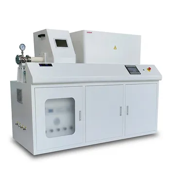
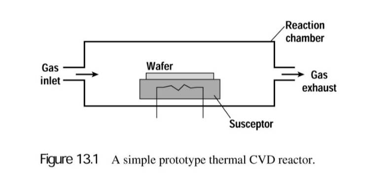
Chemical Vapor Deposition (CVD) is a sophisticated chemical phenomenon where a material is meticulously deposited onto another material using a film of a different substance. This process typically involves introducing gaseous raw materials into a precisely controlled reaction chamber. Within this chamber, the gases undergo a series of chemical reactions, resulting in the formation of a new material that is then deposited onto the surface of a wafer or substrate.
The essence of CVD lies in its ability to manipulate the chemical environment to achieve the desired deposition outcome. The materials involved in the process are usually in volatile form, ensuring that they can readily react with the substrate to form the intended deposit. This method is not only versatile but also highly efficient, capable of producing a wide array of materials, including silicon, carbon, nitrides, carbides, oxides, and even synthetic diamonds.
During the CVD process, several by-products are inevitably produced. These by-products, which are typically in gaseous form, escape from the reaction chamber, ensuring that they do not interfere with the deposition process. The use of gases as reactants in CVD offers significant advantages, such as the ability to achieve high purity levels—often ranging from 99.99% to 99.999%—and the formation of materials with densities close to 100%.
In the realm of semiconductors, CVD plays a pivotal role in the fabrication of dry semiconductor devices and the deposition of materials like amorphous SiO₂, silicon germanium, and tungsten. Its versatility and reliability make it the preferred choice for a myriad of applications, from the production of synthetic diamonds to the creation of advanced coatings and fibers.
Types of CVD Processes
Chemical Vapor Deposition (CVD) encompasses a diverse array of processes, each tailored to meet specific industrial and application-driven demands. The spectrum of CVD techniques includes:
-
Atmospheric Pressure Chemical Vapour Deposition (APCVD): This method operates at atmospheric pressure, eliminating the need for vacuum pumps but often resulting in slower deposition rates compared to low-pressure methods.
-
Low Pressure Chemical Vapour Deposition (LPCVD): LPCVD employs a vacuum pump to draw gas through the deposition chamber, enabling a more uniform deposition rate and reducing gas-phase reactions. This method is particularly advantageous for achieving precise and consistent film thicknesses.
-
Metal-Organic Chemical Vapour Deposition (MOCVD): Utilizing organic compounds and hydrides, MOCVD facilitates the growth of various compound semiconductors through vapor phase epitaxy, making it essential for advanced semiconductor applications.
-
Plasma Assisted Chemical Vapour Deposition (PACVD) or Plasma Enhanced Chemical Vapour Deposition (PECVD): These techniques excite gases to produce low-temperature plasma, significantly enhancing chemical activity and enabling epitaxial growth at reduced temperatures.
-
Laser Chemical Vapour Deposition (LCVD): LCVD employs laser energy to excite chemical vapor reactions, facilitating thin film deposition at lower temperatures and offering precise control over the deposition process.
-
Photochemical Vapour Deposition (PCVD): PCVD leverages light energy to initiate chemical reactions, offering a unique approach to film deposition with potential applications in specialized industries.
-
Chemical Vapour Infiltration (CVI): CVI is particularly useful for creating composites by infiltrating pre-formed porous substrates with reactive gases, leading to the formation of dense, high-performance materials.
-
Chemical Beam Epitaxy (CBE): CBE involves directing a focused beam of reactive chemicals onto a substrate, enabling the precise control of film composition and structure for advanced semiconductor devices.
These various CVD processes are not only distinguished by their operational parameters but also by their reactor configurations and gas flow directions. For instance, horizontal tube reactors are commonly used in many CVD processes, ensuring efficient gas flow towards the substrate and facilitating uniform deposition.
Advanced CVD Techniques
Plasma Enhanced Chemical Vapor Deposition (PECVD)
Plasma Enhanced Chemical Vapor Deposition (PECVD) represents a significant advancement in the field of chemical vapor deposition (CVD) techniques. Unlike traditional CVD methods that rely solely on substrate temperature to drive chemical reactions, PECVD leverages the power of plasma to enhance the deposition process. This plasma, generated by exciting gas molecules, significantly boosts chemical activity, enabling the formation of thin films at much lower temperatures compared to conventional CVD processes.
| Feature | PECVD | Conventional CVD |
|---|---|---|
| Energy Source | Plasma energy | Thermal energy |
| Processing Temperature | 200-400°C | 425-900°C |
| Deposition Rate | Higher | Lower |
| Film Quality | Good uniformity | Variable |
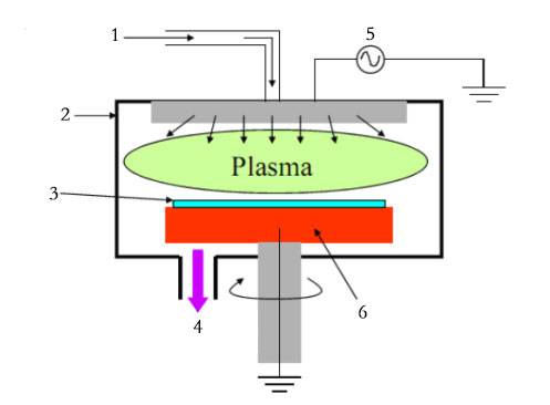
The energetic electrons within the plasma play a crucial role in activating the CVD process, thereby reducing the need for high substrate temperatures. This makes PECVD particularly advantageous for depositing high-quality films on temperature-sensitive substrates such as optical glass, silicon, quartz, and stainless steel. Common materials deposited using PECVD include silicon nitride, amorphous silicon, and microcrystalline silicon, all of which require precise control and uniformity in their film properties.
By utilizing plasma energy, PECVD not only lowers the processing temperature but also enhances the deposition rate, making it a versatile and efficient technique for various industrial applications. This method is particularly favored in the semiconductor industry for its ability to produce uniform, high-quality thin films at reduced operational costs and with greater process control.
High-density Plasma Chemical Vapor Deposition (HDP CVD)
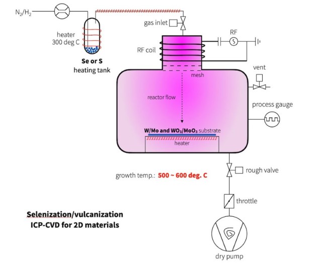
High-density Plasma Chemical Vapor Deposition (HDP-CVD) employs an inductively coupled plasma (ICP) source to achieve superior plasma density and quality compared to conventional Plasma Enhanced Chemical Vapor Deposition (PECVD) methods. This advanced technique operates at lower deposition temperatures, making it particularly effective for applications requiring precise control over the deposition process.
One of the key advantages of HDP-CVD is its ability to independently regulate ion flux and energy, which significantly enhances the filling capabilities of trenches and holes, especially those with high aspect ratios. This capability addresses the limitations of PECVD, which often resulted in pinch-offs and voids when filling narrow gaps smaller than 0.8 microns.
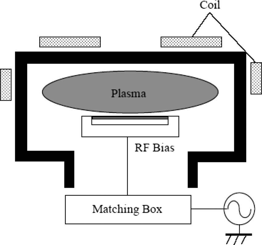
Moreover, the versatility of HDP-CVD extends beyond deposition. The same system can be reconfigured to function as an Inductively Coupled Plasma Reactive Ion Etching (ICP-RIE) tool, providing a dual-use capability that is particularly beneficial in scenarios where budget constraints or limited space are factors. This dual functionality not only optimizes resource utilization but also simplifies the overall process workflow in semiconductor fabrication.
Microwave Plasma Chemical Vapor Deposition (MPCVD)
Microwave Plasma Chemical Vapor Deposition (MPCVD) is a sophisticated technique used for synthesizing high-quality hard films and large-sized single-crystal diamonds. This method leverages microwave radiation to generate high-energy plasma within a reactor chamber, creating an environment conducive to diamond formation. The plasma, a mixture of electrons, ions, neutral particles, and molecular fragments, is characterized by its high electron density at the center, which gradually diminishes towards the edges.
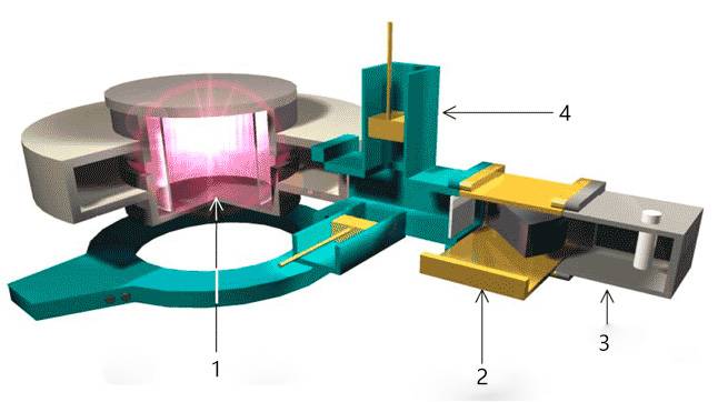
The primary mechanism behind MPCVD involves the dissociation of reaction gases, such as a mixture of methane (CH₄) and hydrogen (H₂), through electron impact. This dissociation generates reactive carbonaceous species and an abundance of atomic/molecular hydrogen near the substrate, fostering the deposition of diamond films. The process is unique in that the electrons, energized by the oscillating electric field of microwave radiation, can reach temperatures up to 5273 K, while the gas temperature remains relatively low at around 1073 K, especially in low-pressure synthesis methods.
Commonly employed microwave frequencies for this process include 2.45 GHz and 915 MHz, which are optimized to ensure efficient plasma generation and stable diamond film growth. The controlled environment within the MPCVD reactor, combined with the precise energy input, allows for the deposition of high-quality diamond films with exceptional properties, making MPCVD a preferred method in various industrial applications.
Microwave Electron Cyclotron Resonance Plasma Chemical Vapor Deposition (ECR-MPCVD)
Microwave Electron Cyclotron Resonance Plasma Chemical Vapor Deposition (ECR-MPCVD) represents a sophisticated technique in the realm of chemical vapor deposition (CVD) that leverages the cyclotron resonance effect of electrons within microwave and magnetic fields. This method is instrumental in generating a highly active and dense plasma under vacuum conditions, which is pivotal for the preparation of high-quality diamond films at relatively low temperatures[^4].
The core mechanism of ECR-MPCVD involves the excitation of gas molecules through electromagnetic waves, typically operating at a frequency of 2450 MHz. By modulating the energy of these electromagnetic waves, the energy and lifespan of the gas particles, once decomposed, can be precisely controlled. This control has a direct bearing on the formation and surface processing of the deposited films, ultimately influencing the structural integrity, properties, and stability of the resultant diamond films[^4].
In essence, ECR-MPCVD not only enhances the plasma density but also optimizes the conditions necessary for the synthesis of superior diamond films. This technique is particularly advantageous for applications requiring high-quality, large-sized single-crystal diamonds, where the precise control over plasma parameters and deposition conditions is paramount.
Ultra-high Vacuum Chemical Vapor Deposition (UHV/CVD)
Ultra-high vacuum chemical vapor deposition (UHV/CVD) is a sophisticated thin film technology that operates under conditions of extremely low pressure, typically below 10^-6 Pa (10^-8 Torr). This method is particularly renowned for its ability to produce high-quality submicron crystalline films, nanostructured materials, and advanced silicon-based devices, such as high-speed high-frequency components and nanoelectronic devices.
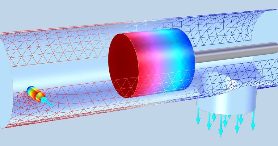
UHV/CVD was developed in the late 1980s and has since become a cornerstone in the fabrication of single crystal thin films. Unlike traditional vapor phase epitaxy, UHV/CVD employs low-pressure and low-temperature growth conditions. This approach significantly mitigates the solid-state diffusion of doping sources and suppresses the three-dimensional growth of epitaxial films, leading to more controlled and uniform film deposition.
One of the standout materials that can be synthesized through UHV/CVD is graphene. The ultra-high vacuum environment of the UHV/CVD system plays a crucial role in this process. By maintaining a vacuum below 10^-6 Pa, the system effectively prevents the oxidation of the silicon substrate surface and minimizes the incorporation of impurities from reaction gases into the growing film. This pristine environment is essential for achieving the high purity and structural integrity required for advanced electronic and optical applications.
In UHV/CVD, gas transport occurs via molecular flow, a mechanism that ensures minimal molecular collisions. This low frequency of collisions precludes gas-phase chemistry, further enhancing the quality and uniformity of the deposited films. The process involves the interaction of one or more volatile precursors with a substrate under ultra-high vacuum conditions, leading to surface reactions that result in the formation of a deposit. This technique is particularly advantageous for depositing chemically active single crystal thin films on high substrate surfaces, making it indispensable in the semiconductor industry for the production of cutting-edge devices.
Low-pressure Chemical Vapor Deposition (LPCVD)
Low-pressure Chemical Vapor Deposition (LPCVD) operates by significantly reducing the reactor pressure to approximately 133 Pa or less, a condition that markedly enhances the efficiency of the deposition process. This reduction in pressure fosters an environment where the gas diffusion coefficient and mean free path are increased, thereby improving the uniformity of the deposited films. The enhanced gas diffusion within the reactor chamber leads to better control over film properties such as resistivity and the ability to fill trenches effectively.
Moreover, the lower pressure environment accelerates the gas transport rate, allowing impurities and reaction by-products to be swiftly removed from the reaction zone. This rapid removal process not only improves the overall purity of the deposited film but also mitigates issues such as self-doping, thereby enhancing the quality and efficiency of the deposition process. Additionally, LPCVD does not necessitate the use of carrier gases, which significantly reduces the risk of particle contamination, making it a preferred method in the high-value semiconductor industry for the deposition of thin films.
LPCVD is particularly advantageous in applications such as the production of resistors, capacitor dielectrics, Micro-Electro-Mechanical Systems (MEMS), and anti-reflective coatings. The controlled low-pressure conditions, combined with optimized precursor delivery systems, ensure that the deposited films exhibit superior properties, making LPCVD a key technology in advanced semiconductor manufacturing.
Thermal Chemical Vapor Deposition (TCVD)
Thermal Chemical Vapor Deposition (TCVD) is a sophisticated method of vapor phase growth that harnesses high temperatures to catalyze chemical reactions. This technique is pivotal in various TCVD technologies, including Metal Organic Chemical Vapor Deposition (MOCVD), Chloride Chemical Vapor Deposition, and Hydride Chemical Vapor Deposition, all of which fall under the umbrella of thermal chemical vapor deposition.
TCVD can be further categorized based on the nature of its chemical reactions:
-
Chemical Transport Method: In this approach, the substance forming the thin film reacts with another solid or liquid substance in the source area, generating a gas. This gas is then transported to the growth area at a specific temperature, where it undergoes a reverse thermal reaction to produce the desired material. The forward reaction represents the thermal process during transport, while the reverse reaction signifies the thermal process during crystal growth.
-
Pyrolysis Method: This method involves transporting certain volatile substances containing film elements to the growth area. Here, these substances undergo thermal decomposition reactions to yield the required materials. The growth temperature for this method typically ranges between 1000-1050 degrees Celsius.
The versatility and precision of TCVD make it an indispensable tool in the semiconductor and thin film deposition industries, offering a robust platform for creating high-quality, structurally sound materials.
High Temperature Chemical Vapor Deposition (HTCVD)
High Temperature Chemical Vapor Deposition (HTCVD) is an indispensable technique for the growth of silicon carbide crystals, a process that demands extreme temperatures to achieve the desired results. In this method, silicon carbide crystals are cultivated within a closed reactor, where external heating is meticulously controlled to maintain the reaction chamber at a temperature range of 2000°C to 2300°C. This high-temperature environment is essential for the intricate chemical reactions that occur on the surface of the substrate material.
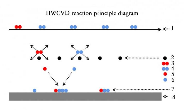
The HTCVD process can be broken down into several critical steps:
-
Introduction of Mixed Reaction Gas: The process begins with the introduction of a precisely mixed reaction gas into the reactor. This gas mixture is designed to facilitate the desired chemical reactions necessary for crystal growth.
-
High-Temperature Decomposition: Once the reaction gas reaches the substrate surface, it undergoes decomposition at the extreme temperatures within the reactor. This decomposition is a pivotal step that sets the stage for the subsequent chemical reactions.
-
Surface Chemical Reactions: The decomposed reaction gas then undergoes a series of chemical reactions on the substrate surface. These reactions are responsible for the formation of a solid crystal film, which is the foundational layer of the silicon carbide crystal.
-
Crystal Film Growth: As the solid product is continuously detached and moved away from the substrate surface, fresh reaction gas is introduced to replace it. This continuous flow of gas ensures that the crystal film layer grows steadily and uniformly.
-
Thermodynamics and Gas Transport: The success of the HTCVD process hinges on the interplay between thermodynamics and gas transport mechanisms. These factors govern how effectively the reaction gases interact with the substrate and how efficiently the solid products are removed to allow for continued growth.
The high temperatures involved in HTCVD not only enhance the rate of chemical reactions but also ensure the formation of high-quality, crystalline films. This makes HTCVD a crucial technique for applications requiring robust and high-performance materials, such as in the semiconductor industry where silicon carbide is prized for its exceptional thermal and electrical properties.
Medium-temperature Chemical Vapor Deposition (MTCVD)
Medium-temperature Chemical Vapor Deposition (MTCVD) is a critical technology in the hard coating processes of the cemented carbide tool industry. This method has been instrumental in enhancing the durability and performance of cutting tools, particularly in high-speed, high-efficiency cutting applications. MTCVD's ability to deposit robust coatings at temperatures ranging from 700°C to 900°C has made it a preferred choice for addressing the challenges of low tool life in demanding machining operations such as heavy cutting of alloy steel and dry cutting.
The MTCVD process is characterized by specific operational parameters: the deposition temperature typically ranges from 700°C to 900°C, while the deposition reaction pressure is maintained between 2X10³ Pa and 2X10⁴ Pa. The primary reaction gases used in the process are a mixture of CH₃CN, TiCl₄, and H₂, with a typical gas ratio of 0.01:0.02:1. The deposition time can vary from 1 to 4 hours, depending on the desired coating thickness and properties.
MTCVD's significance in the industry is underscored by its successful integration into the production lines of major carbide tool manufacturers. By combining MTCVD with High-temperature Chemical Vapor Deposition (HTCVD), these companies have developed new super carbide coating materials that have effectively mitigated the issue of low tool life in high-strength machining environments. This dual approach has garnered widespread attention and has led to significant advancements in the coated carbide tool industry, demonstrating remarkable practical effects.
In summary, MTCVD stands out as a pivotal technology in the cemented carbide tool industry, offering a reliable solution to enhance tool durability and performance in high-stress machining conditions. Its precise operational parameters and successful industrial applications highlight its importance in modern manufacturing processes.
Metal Organic Chemical Vapor Deposition (MOCVD)
Metal Organic Chemical Vapor Deposition (MOCVD) is a sophisticated epitaxial growth technology that has revolutionized the fabrication of compound semiconductors. This method leverages the vapor phase epitaxy process, where organic compounds of group III and II elements, along with hydrides of group V and VI elements, serve as the primary source materials. These materials are introduced into a reaction chamber, where they undergo thermal decomposition to form thin, single-crystal layers on a substrate.
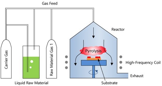
The versatility of MOCVD is evident in its ability to grow a wide array of compound semiconductors, including III-V and II-VI materials, as well as their multilayered solid solutions. The process is particularly advantageous for creating complex heterostructures, superlattice materials, and quantum well structures, which are crucial for advanced semiconductor devices.
One of the key benefits of MOCVD is the precise control it offers over the composition and dopant concentration of the deposited layers. By accurately regulating the flow rate and on/off timing of the gaseous sources, MOCVD enables the growth of ultra-thin layers with specific properties. Additionally, the rapid gas flow within the reaction chamber allows for swift adjustments in the composition of multiple compounds, minimizing the risk of memory effects and ensuring sharp interfaces between different layers.
Compared to other epitaxial growth techniques, MOCVD stands out due to its ability to handle a wide range of materials and its adaptability in producing high-quality, complex semiconductor structures. This makes it an indispensable tool in the semiconductor industry for the development of next-generation electronic and optoelectronic devices.
Laser-induced Chemical Vapor Deposition (LCVD)
Laser-induced Chemical Vapor Deposition (LCVD) is a sophisticated method of depositing thin films by harnessing the photon energy of a laser beam to stimulate and facilitate chemical vapor phase reactions. In this process, the laser beam's energy decomposes molecules in the gas phase, activating atoms to form thin films on the substrate. This technique notably lowers the substrate temperature compared to conventional Chemical Vapor Deposition (CVD), preventing the disruption of impurity distribution within the substrate and enabling the synthesis of thin films on substrates that are unable to withstand high temperatures. Unlike plasma CVD methods, LCVD avoids the damage caused by high-energy particle irradiation, enhancing the quality and integrity of the deposited films.
LCVD operates by locally decomposing reagent gases through the heat generated from a focused laser beam, resulting in metallic and ceramic depositions on a substrate. The localized nature of laser heating allows for precise patterning and direct writing capabilities by moving the focused laser beam relative to the substrate. This localized heating is a key advantage, enabling finer resolutions and more controlled deposition patterns.
LCVD is further categorized into two primary types: photolytic and pyrolytic. In photolytic LCVD, the energy from the focused laser beam is absorbed by the reagent gases, causing their decomposition and subsequent deposition of solid atoms or molecules onto the substrate. The laser wavelengths used in this process are material-dependent, with typical applications involving UV lasers such as Ar+, ArF, and KrF. However, the absorption of laser energy may extend along the beam path rather than being confined to the focal point, potentially reducing resolution and increasing feature sizes.
Conversely, pyrolytic LCVD involves the laser beam irradiating specific locations on the substrate where material deposition is desired. This irradiation locally increases the substrate temperature, triggering gas decomposition and the formation of a solid layer. Typical lasers used in pyrolytic LCVD include continuous wave infrared lasers like CO2 and Nd:YAG. The localized heating in this method allows for finer resolutions, with capabilities down to 5 μm, making it particularly advantageous for applications requiring high precision and detailed patterning.
Related Products
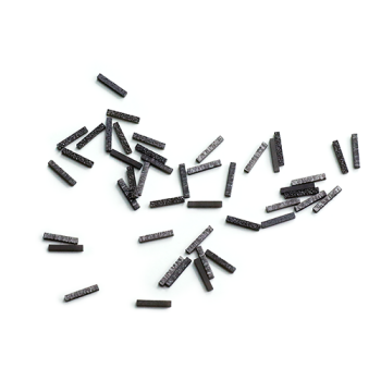
- CVD Diamond Dressing Tools for Precision Applications
- Multi Heating Zones CVD Tube Furnace Machine Chemical Vapor Deposition Chamber System Equipment
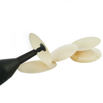
- CVD Diamond Domes for Industrial and Scientific Applications
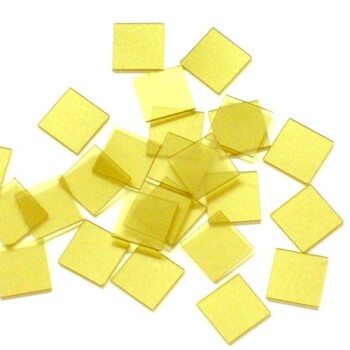
- CVD Diamond for Thermal Management Applications
- Chemical Vapor Deposition CVD Equipment System Chamber Slide PECVD Tube Furnace with Liquid Gasifier PECVD Machine
