Introduction to PECVD in MEMS
Role of PECVD in MEMS Devices
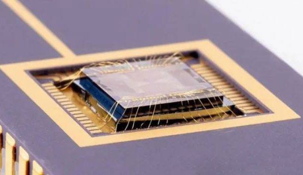
PECVD (Plasma-Enhanced Chemical Vapor Deposition) is indispensable for the fabrication of high-quality silicon oxide and nitride films, which are critical components in various layers of MEMS (Micro-Electro-Mechanical Systems) devices. This technique is favored for its ability to deposit films at relatively low temperatures, ensuring that delicate structures within MEMS devices are not compromised by excessive heat.
The significance of PECVD in the semiconductor industry extends beyond MEMS to include a wide array of applications such as microelectronic devices, photovoltaic cells, and display panels. Its advantages include excellent film uniformity, high throughput, and the capability to process materials at temperatures that are compatible with existing metal layers within devices. This makes PECVD particularly suitable for the final stages of device fabrication where traditional thermal CVD processes would be too harsh.
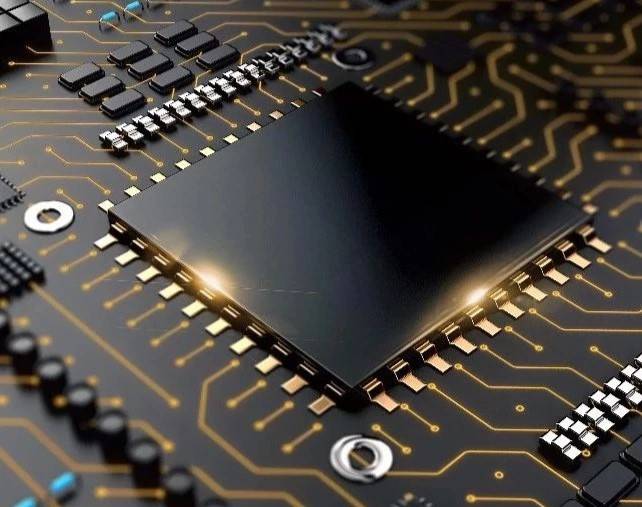
In PECVD processes, glow-discharge plasmas are maintained within chambers, facilitating simultaneous vapor-phase chemical reactions and film deposition. This method was developed in response to the stringent demands of semiconductor technology, mirroring the evolution of other plasma-based processes like sputtering and etching. Early commercial applications of PECVD notably included the low-temperature deposition of silicon nitride films, which were used for the passivation and encapsulation of fully fabricated microelectronic devices. The ability to deposit silicon nitride at temperatures below 300°C was a game-changer, as it allowed for the protection of sensitive components without causing thermal degradation.
As the demand for advanced electronic devices continues to escalate, the role of PECVD in the semiconductor industry is poised to become even more pivotal. Its ability to balance film quality with process efficiency makes it an essential tool for the future of MEMS and other micro-fabrication technologies.
Comparison with Other Deposition Methods
PECVD (Plasma-Enhanced Chemical Vapor Deposition) stands out among other deposition methods due to its unique capabilities in temperature control and compatibility with existing metal layers. Unlike traditional CVD (Chemical Vapor Deposition) methods, PECVD operates at lower temperatures, typically ranging from 150°C to 400°C, which is crucial for preserving the integrity of pre-existing metal structures in MEMS devices. This temperature range allows for the deposition of high-quality silicon oxide and nitride films without causing thermal damage to sensitive components.
Moreover, PECVD's ability to control the deposition process through adjustable parameters such as RF power, gas flow rates, and chamber pressure further enhances its versatility. This flexibility ensures that the deposited films can be tailored to meet specific requirements for electrical, mechanical, and thermal properties, making PECVD an ideal choice for the intricate needs of MEMS fabrication.
| Deposition Method | Temperature Range | Compatibility with Metal Layers | Adjustability |
|---|---|---|---|
| PECVD | 150°C - 400°C | High | High |
| Traditional CVD | 400°C - 1000°C | Low | Low |
In summary, PECVD's low-temperature operation and high adjustability make it superior for MEMS devices that require precise control over film properties and protection of existing metal layers.
Components of PECVD Equipment
RF Electrode and Wafer Electrode
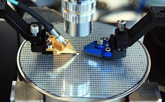
In the context of PECVD (Plasma-Enhanced Chemical Vapor Deposition) for MEMS (Micro-Electro-Mechanical Systems) devices, the RF (Radio Frequency) electrode and wafer electrode play pivotal roles in the deposition process. The RF electrode is specifically designed to decompose the raw material gases into a plasma state. This plasma, rich in reactive species, is essential for the uniform and controlled deposition of silicon oxide and nitride films. The RF electrode's ability to ionize gases efficiently ensures that the resulting plasma has the necessary energy to facilitate chemical reactions at lower temperatures, which is crucial for maintaining the structural integrity of MEMS devices.
On the other hand, the wafer electrode serves a dual purpose: it acts as a carrier for the wafer and provides the necessary heating to maintain optimal deposition conditions. The heating function of the wafer electrode is critical as it helps in controlling the temperature of the wafer, which in turn influences the growth rate and quality of the deposited films. By maintaining a consistent temperature, the wafer electrode ensures that the film properties, such as thickness and uniformity, are optimized. This dual functionality of the wafer electrode underscores its importance in the PECVD process, making it an indispensable component for achieving high-quality coatings in MEMS devices.
Vacuum Pump and Raw Material Gas
The vacuum pump in PECVD equipment plays a pivotal role in controlling the gas flow within the chamber, ensuring that the environment remains conducive to the decomposition and subsequent formation of the desired films. This critical component not only maintains the necessary vacuum levels but also aids in the decomposition of gases, facilitating the efficient creation of plasma.
Raw material gases, such as silane (SiH4), nitrous oxide (N2O), and nitrogen (N2), are indispensable for the film formation process. These gases are carefully introduced into the chamber and subjected to the energy from the RF electrode, breaking down into their constituent atoms and molecules. This plasma state is essential for the deposition of high-quality silicon oxide and nitride films on the MEMS devices.
| Gas | Role in Film Formation |
|---|---|
| SiH4 | Provides silicon atoms for forming silicon-based films. |
| N2O | Supplies oxygen and nitrogen for the creation of silicon oxide and nitride films. |
| N2 | Enhances the nitrogen content in the films, influencing their mechanical properties. |
The precise control of gas flow and the effective decomposition of these raw materials are key to achieving uniform and high-quality films. Any deviation in the gas composition or flow rate can lead to variations in film properties, thereby affecting the overall performance and reliability of the MEMS devices.
Process Control and Optimization
Film Growth and Quality Control
The growth rate of the film, the concentration of the gases used, and the activation energy required are all critical factors that significantly influence both the thickness and the quality of the film. These factors are meticulously controlled through the application of RF power and the regulation of wafer temperature.
- Growth Rate: The rate at which the film grows is directly proportional to the RF power applied. Higher RF power accelerates the decomposition of the raw material gases into plasma, thereby speeding up the deposition process.
- Gas Concentration: The concentration of gases like SiH4, N2O, and N2 plays a pivotal role. Optimal concentrations ensure that the film is not only thick enough but also possesses the desired properties such as density and uniformity.
- Activation Energy: This is the energy required to initiate and sustain the chemical reactions necessary for film formation. Controlling the activation energy through RF power and wafer temperature ensures that the reactions proceed efficiently without compromising the film's integrity.
By fine-tuning these parameters, manufacturers can achieve films with precise thickness and superior quality, which are essential for the performance and reliability of MEMS devices.
Parameter Optimization for Desired Properties
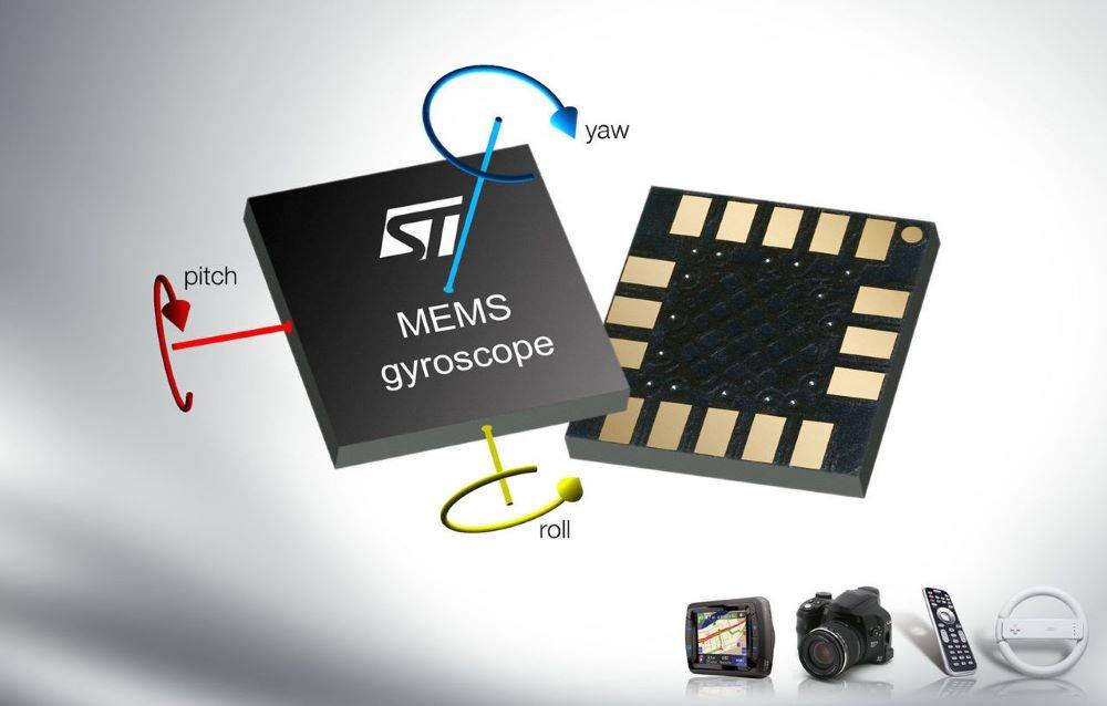
Optimizing the parameters in a Plasma-Enhanced Chemical Vapor Deposition (PECVD) process is essential for achieving the desired film properties in Micro-Electro-Mechanical Systems (MEMS) devices. Key parameters such as the silane/nitrous oxide ratio, RF power, nitrogen flow, chamber pressure, and lower plate temperature play a pivotal role in this optimization process. Each of these parameters directly influences the film's characteristics, including its thickness, uniformity, and mechanical properties.
The silane/nitrous oxide ratio is particularly critical as it affects the chemical composition of the deposited film, influencing its dielectric properties and stability. Adjusting this ratio can fine-tune the film's ability to withstand electrical stresses and mechanical strains, which are crucial for the operational reliability of MEMS devices.
RF power is another significant factor, as it controls the energy input into the plasma, thereby affecting the rate of film growth and the quality of the deposited film. Higher RF power generally increases the growth rate but can also lead to the formation of defects if not properly controlled. Balancing RF power with other parameters ensures a high-quality, defect-free film.
Nitrogen flow, often used to stabilize the plasma and control the film's stoichiometry, is another parameter that requires careful optimization. Proper nitrogen flow ensures uniform film deposition and prevents the formation of unwanted compounds, such as silicon nitride, which can compromise the film's dielectric properties.
Chamber pressure and lower plate temperature are also critical in the PECVD process. Chamber pressure affects the mean free path of the gas molecules, influencing the uniformity and density of the deposited film. Lower plate temperature, on the other hand, controls the substrate's heating, which is essential for promoting the chemical reactions necessary for film formation.
In summary, the interplay between these parameters is crucial for achieving the desired film properties in MEMS devices. Optimizing each parameter within its appropriate range ensures the production of high-quality silicon oxide and nitride films, which are essential for the reliable operation of MEMS devices.
Related Products
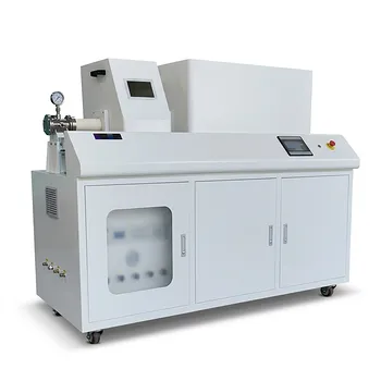
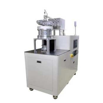
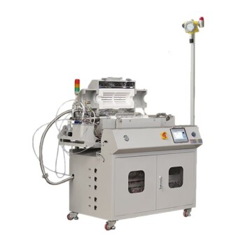
- Inclined Rotary Plasma Enhanced Chemical Vapor Deposition PECVD Equipment Tube Furnace Machine
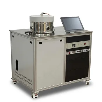
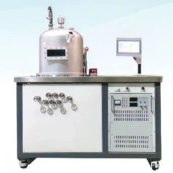
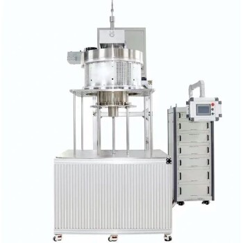
- RF PECVD System Radio Frequency Plasma-Enhanced Chemical Vapor Deposition RF PECVD
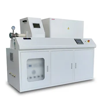
- Inclined Rotary Plasma Enhanced Chemical Vapor Deposition PECVD Equipment Tube Furnace Machine
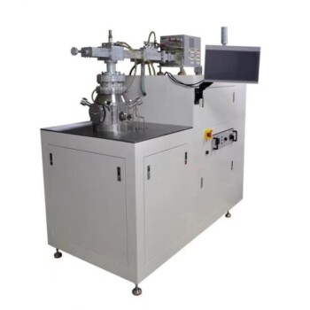
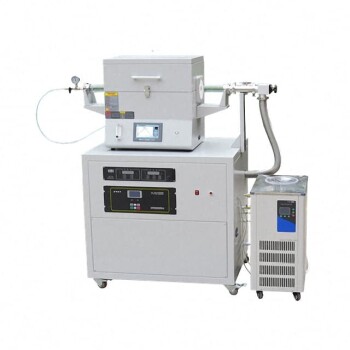
- Chemical Vapor Deposition CVD Equipment System Chamber Slide PECVD Tube Furnace with Liquid Gasifier PECVD Machine
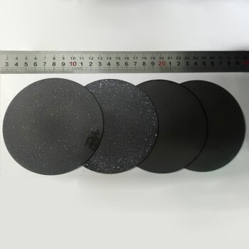
- Custom CVD Diamond Coating for Lab Applications
