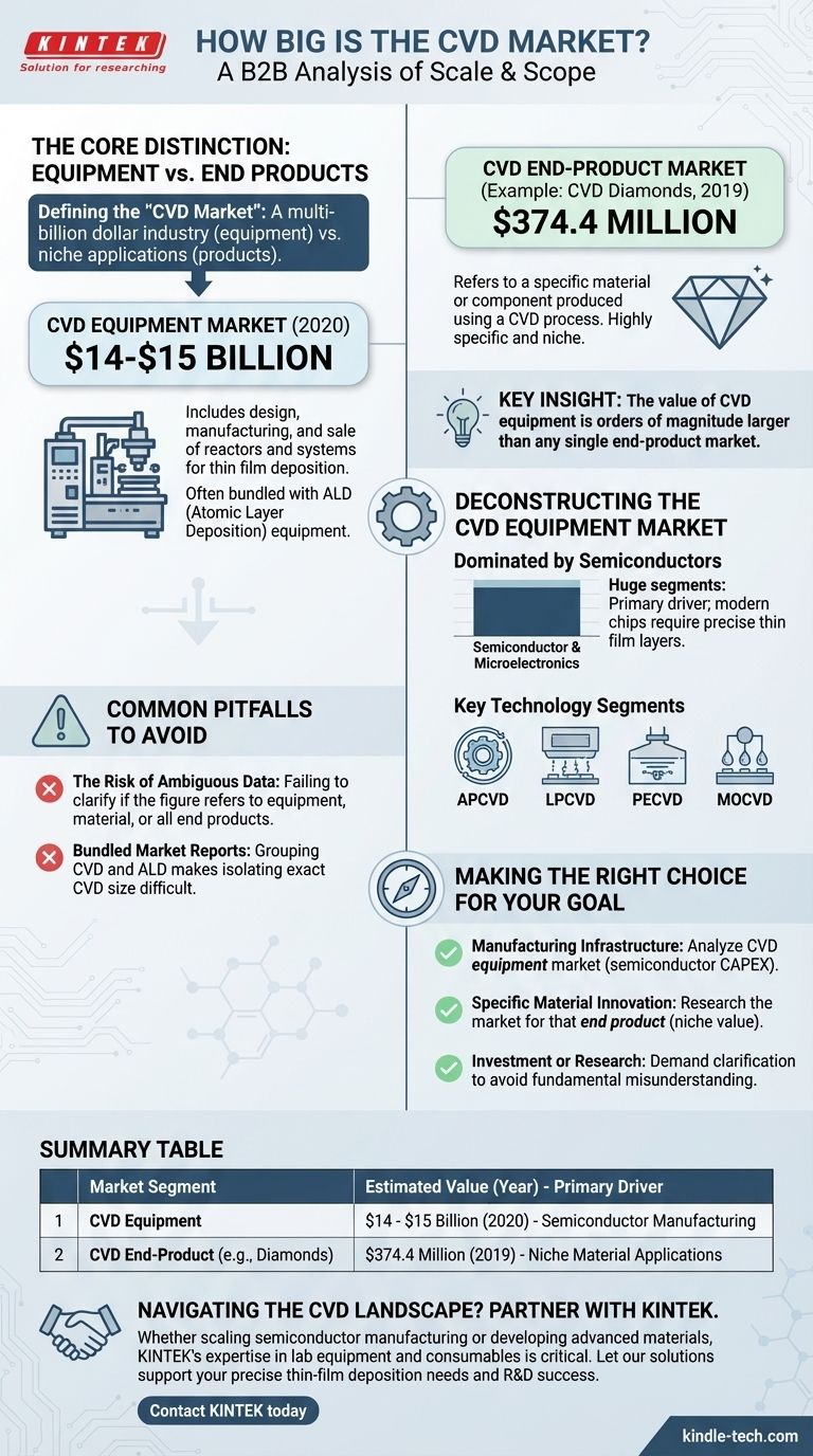
Defining the "CVD market" is the first critical step, as the term can be ambiguous. The market for the equipment used in Chemical Vapor Deposition (CVD), often reported alongside ALD equipment, was valued at approximately $14-$15 billion in 2020. In contrast, the market for a specific product made with this technology, such as CVD diamonds, was valued at a much smaller $374.4 million in 2019, illustrating a critical distinction.
The term "CVD market" is misleading without context. The market for CVD equipment is a multi-billion dollar industry dominated by semiconductor manufacturing. Markets for specific products made with CVD are orders of magnitude smaller and represent niche applications.
The Core Distinction: Equipment vs. End Products
To understand the financial landscape of CVD, you must differentiate between the machinery that performs the process and the goods that are created by it. These are two vastly different markets in scale and scope.
The CVD Equipment Market
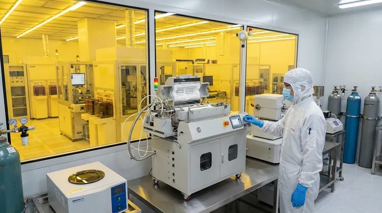
The largest and most commonly cited figure refers to the CVD equipment market. This encompasses the design, manufacturing, and sale of the reactors and systems that companies use to deposit thin films.
This market was valued at $14-$15 billion in 2020, a figure that typically includes the related Atomic Layer Deposition (ALD) equipment market.
The CVD End-Product Market
This refers to the market for a specific material or component produced using a CVD process. These markets are highly specific and much smaller.
A clear example is the CVD diamond market, valued at approximately $374.4 million in 2019. This figure represents the value of the synthetic diamonds themselves, not the machines that made them.
Deconstructing the CVD Equipment Market
The high value of the CVD equipment market is almost entirely due to its indispensable role in one specific industry.
Dominated by Semiconductors
The semiconductor and microelectronics industry is the primary driver of the CVD equipment market. Modern computer chips are built layer by layer with incredibly precise thin films, and CVD is a foundational technology for depositing many of these critical layers.
Every major semiconductor fabrication plant requires a significant investment in various types of CVD systems.
Key Technology Segments
The equipment market is not monolithic. It is segmented by the specific type of CVD technology, each suited for different materials and applications.
These segments include:
- Atmospheric Pressure CVD (APCVD)
- Low-Pressure CVD (LPCVD)
- Plasma-Enhanced CVD (PECVD)
- Metal-Organic CVD (MOCVD)
Common Pitfalls to Avoid
When analyzing market data, a lack of specificity can lead to billion-dollar errors in judgment. Understanding the common points of confusion is essential.
The Risk of Ambiguous Data
If a report or individual quotes a "CVD market size," you must immediately ask what is being measured. Is it equipment, a single material, or the total value of all end products containing a CVD-deposited film?
Failing to clarify this point is the most common mistake made when assessing this technology's financial footprint.
Bundled Market Reports (CVD & ALD)
Market analysis firms frequently group CVD and Atomic Layer Deposition (ALD) into a single "thin film deposition equipment" market.
While the technologies are related, they are distinct. This bundling can make it difficult to isolate the exact market size for CVD equipment alone without access to more granular data.
Making the Right Choice for Your Goal
Your interpretation of the market size depends entirely on your strategic objective.
- If your primary focus is on manufacturing infrastructure: You should analyze the CVD equipment market, the multi-billion dollar segment tied directly to semiconductor capital expenditure.
- If your primary focus is on a specific material innovation: You must research the market for that end product (e.g., CVD diamonds, specialized coatings), which will be a smaller, more niche value.
- If your primary focus is on investment or research: Always demand clarification on whether a figure refers to equipment or a specific product to avoid a fundamental misunderstanding of the market's scale.
Understanding this distinction between the tool and the product is the key to accurately assessing the economic landscape of CVD technology.
Summary Table:
| Market Segment | Estimated Value (Year) | Primary Driver |
|---|---|---|
| CVD Equipment | $14 - $15 Billion (2020) | Semiconductor Manufacturing |
| CVD End-Product (e.g., Diamonds) | $374.4 Million (2019) | Niche Material Applications |
Navigating the complex CVD landscape requires the right partner. Whether you are scaling semiconductor manufacturing or developing advanced materials, KINTEK's expertise in lab equipment and consumables is critical for your R&D and production success. Let our solutions help you achieve precise thin-film deposition and drive your innovation forward. Contact KINTEK today to discuss your specific laboratory needs and how we can support your goals.
Visual Guide
Related Products
- Chemical Vapor Deposition CVD Equipment System Chamber Slide PECVD Tube Furnace with Liquid Gasifier PECVD Machine
- HFCVD Machine System Equipment for Drawing Die Nano-Diamond Coating
- Multi Heating Zones CVD Tube Furnace Machine Chemical Vapor Deposition Chamber System Equipment
- CVD Diamond Dressing Tools for Precision Applications
- CVD Diamond Domes for Industrial and Scientific Applications
People Also Ask
- What happens during deposition chemistry? Building Thin Films from Gaseous Precursors
- What is plasma enhanced chemical vapor deposition PECVD equipment? A Guide to Low-Temperature Thin Film Deposition
- What are the processes of vapor phase deposition? Understand CVD vs. PVD for Superior Thin Films
- How are carbon nanotubes grown? Master Scalable Production with Chemical Vapor Deposition
- What is the chemical vapor deposition growth process? Build Superior Thin Films from the Atom Up


