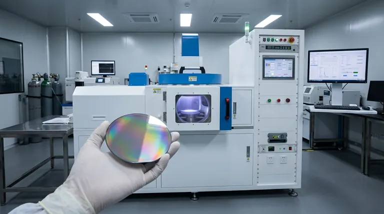
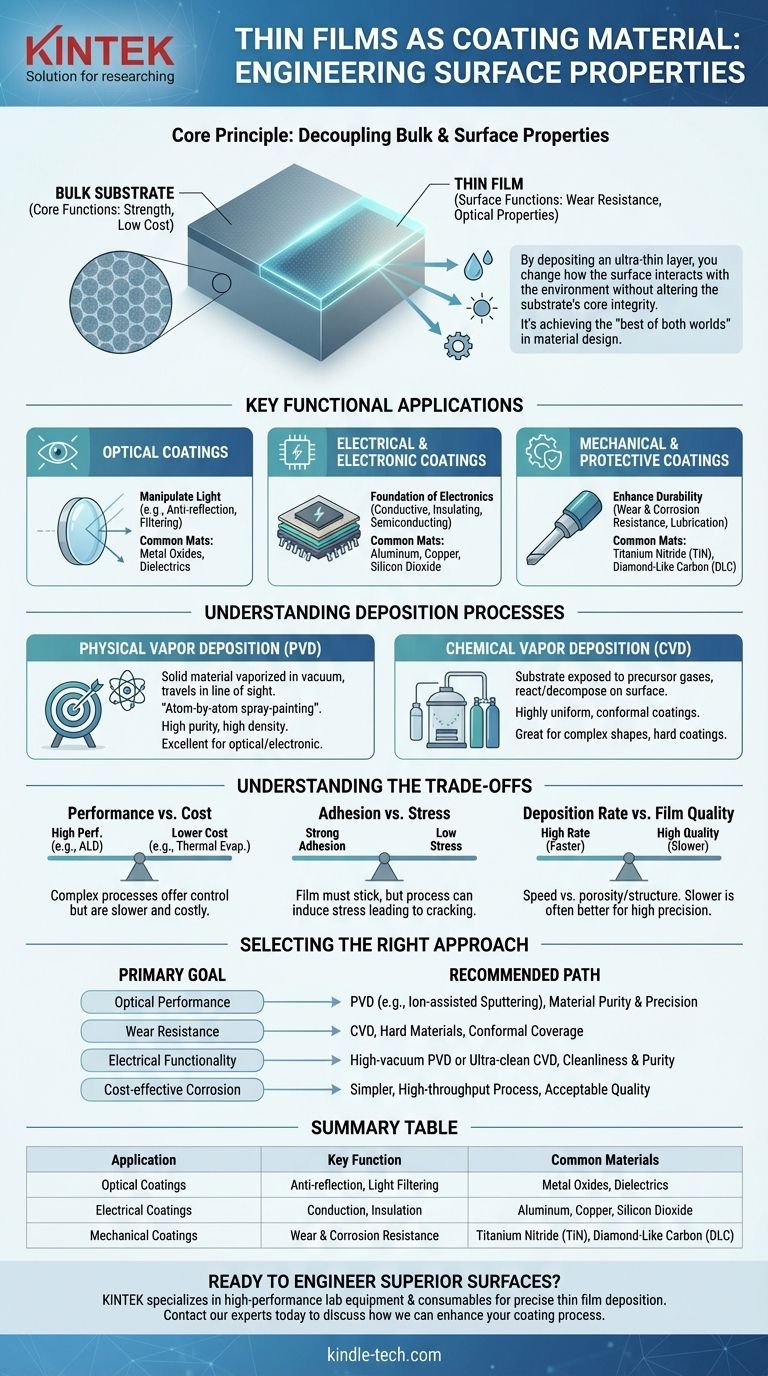
In essence, thin films are used as coatings to apply a new, desirable property to the surface of a bulk material, known as the substrate. By depositing an ultra-thin layer of material—often just a few nanometers to micrometers thick—you can fundamentally change how the substrate interacts with its environment without altering its core structural integrity. This allows engineers to achieve enhanced optical, electrical, mechanical, or chemical performance that the substrate material alone cannot provide.
The true value of a thin film coating is its ability to decouple a material's surface properties from its bulk properties. This allows you to engineer a final product that has the ideal surface function (like anti-reflection) combined with the ideal bulk characteristics (like strength or low cost).
The Core Principle: Why Use a Thin Film Coating?
The decision to use a thin film is a strategic choice to solve a specific engineering problem at the surface level. It’s a method of achieving the "best of both worlds" in material design.
Separating Bulk and Surface Properties
A component's primary function often relies on its bulk material—for example, the strength of a steel tool or the light-transmitting ability of a glass lens.
However, its performance and longevity can be limited by its surface. A thin film allows you to add a specialized function, like wear resistance or water repellency, only where it's needed: on the surface.
Achieving Properties Not Found in a Single Material
Many desired combinations of properties do not exist in any single, monolithic material. You cannot find a material that is both as strong and cheap as steel but also as hard and low-friction as diamond.
By applying a diamond-like carbon (DLC) film onto a steel part, you create a composite system that delivers both the required bulk strength and the desired surface hardness.
Cost-Effectiveness and Material Savings
Many high-performance materials, like gold for electrical contacts or platinum for catalysis, are prohibitively expensive to use as bulk components.
Applying an exceptionally thin film of these precious materials onto a cheaper, stable substrate provides the necessary surface function while dramatically reducing material cost and consumption.
Key Functional Applications of Thin Film Coatings
Thin film coatings are categorized by the function they are designed to perform. This is the most practical way to understand their use.
Optical Coatings
These films manipulate light. By precisely controlling the film's thickness and refractive index, engineers can dictate how light reflects from or transmits through a surface.
Common examples include anti-reflection coatings on eyeglasses and camera lenses, highly reflective coatings for mirrors, and selective filters that only allow specific colors of light to pass through.
Electrical and Electronic Coatings
Thin films are the foundation of the modern electronics industry. They are used to create the complex, layered structures inside microchips.
These films can be conductive (like aluminum or copper wiring), insulating (like silicon dioxide to prevent short circuits), or semiconducting (the basis of transistors). Transparent conductive films are essential for touch screens and solar cells.
Mechanical and Protective Coatings
These coatings are designed to protect the substrate from the physical and chemical environment. The goal is to enhance durability and lifespan.
Hard coatings like titanium nitride (TiN) are applied to cutting tools to improve wear resistance. Other films provide corrosion resistance for parts exposed to harsh chemicals or moisture, or serve as solid lubricants to reduce friction.
Understanding the Deposition Process
How a thin film is applied is just as important as the material itself. The two primary families of deposition are Physical Vapor Deposition and Chemical Vapor Deposition.
Physical Vapor Deposition (PVD)
PVD encompasses methods where a solid material is vaporized in a vacuum and travels in a straight line to condense on the substrate. Think of it as a highly controlled, atom-by-atom spray-painting process.
Common PVD techniques include sputtering and thermal evaporation. PVD is excellent for creating very pure, high-density films and is widely used for optical and electronic applications.
Chemical Vapor Deposition (CVD)
In CVD, the substrate is exposed to one or more volatile precursor gases in a reaction chamber. These gases react or decompose on the substrate's surface to produce the desired film.
CVD is exceptional at creating highly uniform and conformal coatings, meaning it can evenly coat complex, non-flat shapes. It is often used for durable, hard coatings on tools and for creating the high-purity semiconductor layers in microfabrication.
Understanding the Trade-offs
Selecting a thin film coating is not about finding a single "best" solution. It is about balancing competing factors to meet the specific demands of your application.
Performance vs. Cost
More complex deposition processes like atomic layer deposition (ALD) offer unparalleled control over thickness and quality but are slow and expensive. Simpler methods like thermal evaporation are cheaper and faster but offer less control. The required performance level of the final product dictates the acceptable cost of the coating process.
Adhesion vs. Stress
A film is useless if it doesn't stick to the substrate (adhesion). However, the deposition process and material mismatch can create internal stress within the film. High stress can cause the film to crack, peel, or delaminate, completely negating its function. Optimizing the process is a constant balance between maximizing adhesion and minimizing destructive stress.
Deposition Rate vs. Film Quality
In manufacturing, speed is critical. A higher deposition rate means more parts can be coated per hour. However, depositing a film too quickly often leads to a lower-quality, more porous structure with inferior performance. For high-precision applications like optics, a slow, meticulous deposition is non-negotiable.
Selecting the Right Approach for Your Application
Your choice of material, form, and process must be driven by your primary goal.
- If your primary focus is optical performance (e.g., lenses): Prioritize material purity and precise thickness control, often achieved with PVD methods like ion-assisted sputtering.
- If your primary focus is wear resistance (e.g., cutting tools): Select hard materials like nitrides or carbides and use a process like CVD that provides excellent, conformal coverage on complex geometries.
- If your primary focus is electrical functionality (e.g., microchips): The cleanliness of the process and the purity of the material are paramount, making high-vacuum PVD or ultra-clean CVD essential.
- If your primary focus is cost-effective corrosion protection (e.g., fasteners): A simpler, high-throughput process might be sufficient, even if the resulting film quality is not as perfect as in an optical coating.
Ultimately, using a thin film is a powerful act of engineering a material's surface to solve a problem the bulk material cannot.
Summary Table:
| Application | Key Function | Common Materials |
|---|---|---|
| Optical Coatings | Anti-reflection, Light Filtering | Metal Oxides, Dielectrics |
| Electrical Coatings | Conduction, Insulation | Aluminum, Copper, Silicon Dioxide |
| Mechanical Coatings | Wear & Corrosion Resistance | Titanium Nitride (TiN), Diamond-Like Carbon (DLC) |
Ready to engineer superior surface properties for your materials? KINTEK specializes in high-performance lab equipment and consumables for precise thin film deposition. Whether you're developing optical components, durable tools, or advanced electronics, our solutions deliver the purity, adhesion, and uniformity your application demands. Contact our experts today to discuss how we can enhance your coating process and achieve your material goals.
Visual Guide
Related Products
- Aluminized Ceramic Evaporation Boat for Thin Film Deposition
- Electron Beam Evaporation Coating Oxygen-Free Copper Crucible and Evaporation Boat
- Molybdenum Tungsten Tantalum Evaporation Boat for High Temperature Applications
- Aluminum-Plastic Flexible Packaging Film for Lithium Battery Packaging
- Custom CVD Diamond Coating for Lab Applications
People Also Ask
- Why is an alumina boat and Ti3AlC2 powder bed necessary for Ti2AlC sintering? Protect MAX Phase Purity
- What are thin films deposited by evaporation? A Guide to High-Purity Coating
- What is the source of evaporation for thin film? Choosing Between Thermal and E-Beam Methods
- Why is an alumina boat selected for catalyst precursors? Ensure Sample Purity at 1000 °C
- What are the applications of thin films deposition? Unlock New Possibilities for Your Materials


