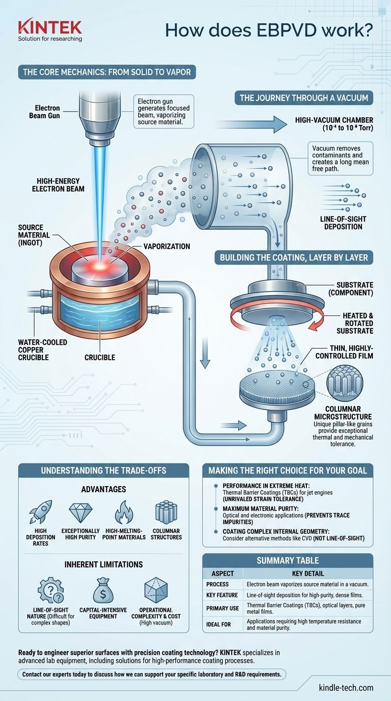
At its core, Electron Beam Physical Vapor Deposition (EBPVD) is a sophisticated coating process that uses a high-energy electron beam to vaporize a source material inside a vacuum. This vapor then travels in a straight line and condenses onto a target component, forming a thin, highly-controlled film. It is essentially a form of "atomic spray painting" used to create advanced material surfaces.
EBPVD is not just about applying a coating; it's about precisely engineering a material's surface structure. The process excels at creating pure, dense, and uniquely structured films, particularly the columnar grain structures essential for components that must withstand extreme thermal and mechanical stress.
The Core Mechanics: From Solid to Vapor
The Electron Beam Gun
The heart of the EBPVD system is the electron gun. It generates a focused, high-energy beam of electrons through a process called thermionic emission, where a tungsten filament is heated until it emits electrons.
These electrons are then accelerated by high voltage and focused using magnetic fields into a tight beam, similar to how an old CRT television worked.
The Source Material and Crucible
This powerful electron beam is directed at a source material, typically a solid ingot or puck, held in a water-cooled copper crucible. The source material is the "paint" you want to apply as a coating.
The intense energy from the electron beam heats a small spot on the ingot's surface to its boiling point, causing it to evaporate directly from a solid or molten state into a vapor. This process provides very high deposition rates and exceptional material purity, as only the source material is heated.
The Journey Through a Vacuum
Why a High Vacuum is Essential
The entire EBPVD process takes place inside a high-vacuum chamber (typically 10⁻⁴ to 10⁻⁶ Torr). This vacuum is critical for two primary reasons.
First, it removes air and other gas molecules that could react with the hot vapor, preventing contamination and ensuring a very pure coating.
Line-of-Sight Deposition
Second, the vacuum creates a long mean free path for the vapor atoms. This means the vaporized atoms can travel from the source to the substrate in a straight line without colliding with other gas molecules.
This "line-of-sight" travel is a defining characteristic of EBPVD, resulting in a highly directional coating process.
Building the Coating, Layer by Layer
Condensation on the Substrate
The component to be coated, known as the substrate, is positioned above the vapor source. When the vapor atoms strike the cooler surface of the substrate, they condense back into a solid state, forming a thin film.
Controlling the Microstructure
The substrate is often heated and precisely rotated and manipulated during deposition. This control is crucial for engineering the final coating's properties.
By controlling temperature and rotation, engineers can create a unique columnar microstructure. These pillar-like grains grow perpendicular to the surface, giving the coating exceptional tolerance to thermal expansion and mechanical strain.
Understanding the Trade-offs
The Advantages of EBPVD
The process offers several distinct benefits. It allows for very high deposition rates, produces coatings of exceptionally high purity, and can be used with high-melting-point materials like ceramics and refractory metals. Its ability to create unique columnar structures is its most significant advantage for certain applications.
Inherent Limitations
However, EBPVD is not without its challenges. The primary drawback is its line-of-sight nature, which makes it difficult to uniformly coat complex shapes with undercuts or internal surfaces.
The equipment is also capital-intensive, and the requirement for a high vacuum adds to the operational complexity and cost.
Making the Right Choice for Your Goal
EBPVD is a specialized tool for demanding applications. Understanding its unique characteristics helps determine if it's the right choice for your specific engineering challenge.
- If your primary focus is performance in extreme heat: EBPVD is the industry standard for creating Thermal Barrier Coatings (TBCs) on jet engine turbine blades, where its columnar structure provides unrivaled strain tolerance.
- If your primary focus is maximum material purity: The process is ideal for optical and electronic applications where even trace impurities in a thin film can degrade performance.
- If your primary focus is coating a complex internal geometry: You should consider alternative methods like Chemical Vapor Deposition (CVD), which is not a line-of-sight process.
Ultimately, choosing EBPVD is a decision to invest in superior surface performance where control over the material's microstructure is paramount.
Summary Table:
| Aspect | Key Detail |
|---|---|
| Process | Electron beam vaporizes source material in a vacuum. |
| Key Feature | Line-of-sight deposition for high-purity, dense films. |
| Primary Use | Thermal Barrier Coatings (TBCs), optical layers, pure metal films. |
| Ideal For | Applications requiring high temperature resistance and material purity. |
Ready to engineer superior surfaces with precision coating technology?
KINTEK specializes in advanced lab equipment, including solutions for high-performance coating processes. Whether you are developing next-generation aerospace components, optical coatings, or electronic thin films, our expertise can help you achieve the material purity and structural control you need.
Contact our experts today to discuss how we can support your specific laboratory and R&D requirements.
Visual Guide
Related Products
- Inclined Rotary Plasma Enhanced Chemical Vapor Deposition PECVD Equipment Tube Furnace Machine
- HFCVD Machine System Equipment for Drawing Die Nano-Diamond Coating
- Vacuum Hot Press Furnace Machine for Lamination and Heating
- 915MHz MPCVD Diamond Machine Microwave Plasma Chemical Vapor Deposition System Reactor
- Laboratory Sterilizer Lab Autoclave Pulse Vacuum Lifting Sterilizer
People Also Ask
- What is the difference between PECVD and CVD? Unlock the Right Thin-Film Deposition Method
- What is PECVD silicon deposition? Achieve Low-Temperature, High-Quality Thin Films
- What materials are deposited in PECVD? Discover the Versatile Thin-Film Materials for Your Application
- How does plasma enhanced CVD work? Achieve Low-Temperature, High-Quality Thin Film Deposition
- What is the difference between CVD and PECVD? Choose the Right Thin-Film Deposition Method