At its core, Low-Pressure Chemical Vapor Deposition (LPCVD) is a fabrication process used to deposit exceptionally high-quality thin films onto a substrate, typically a silicon wafer. It works by introducing reactant gases into a chamber at high temperature and very low pressure. The heat energizes a chemical reaction on the wafer's surface, leaving behind a solid material layer with remarkable uniformity and the ability to perfectly coat complex surface topography.
LPCVD leverages a vacuum environment to create superior thin films. By reducing the pressure, gas molecules move more freely, ensuring that deposition is controlled by the surface reaction itself, not by gas transport. This results in the process's signature benefit: unparalleled conformality.
The Core Principle: A Recipe of Gas, Heat, and Vacuum
Understanding LPCVD requires appreciating the interplay of its three essential components. Each element is precisely controlled to achieve the desired film properties.
The Role of the Vacuum (Low Pressure)
The "Low-Pressure" aspect of LPCVD is its most critical feature. The process chamber is pumped down to a vacuum, typically between 10 to 1000 mTorr (about one-thousandth of atmospheric pressure).
This low pressure significantly increases the mean free path of the gas molecules—the average distance a molecule travels before colliding with another.
With fewer collisions in the gas phase, the reactant molecules can diffuse deep into microscopic trenches and over sharp steps on the wafer surface before reacting. This is the fundamental reason for LPCVD's excellent conformality.
The Importance of High Temperature
LPCVD is a thermally driven process. The wafers are heated in a furnace, usually to temperatures between 500°C and 900°C.
This high temperature provides the activation energy needed to break the chemical bonds in the precursor gases and drive the deposition reaction on the wafer surface.
The temperature must be controlled with extreme precision, as it directly influences the deposition rate and the final properties of the film, such as stress and grain structure.
The Precursor Gases
Precursor gases are the chemical "ingredients" that contain the atoms needed for the final film. They are carefully selected based on the desired material.
Common examples include:
- Silane (SiH₄) for depositing polysilicon.
- Dichlorosilane (SiH₂Cl₂) and Ammonia (NH₃) for depositing silicon nitride (Si₃N₄).
- TEOS (Tetraethyl orthosilicate) for depositing silicon dioxide (SiO₂).
These gases flow into the hot chamber, adsorb onto the wafer surface, decompose, and form the solid film, while gaseous byproducts are pumped away.
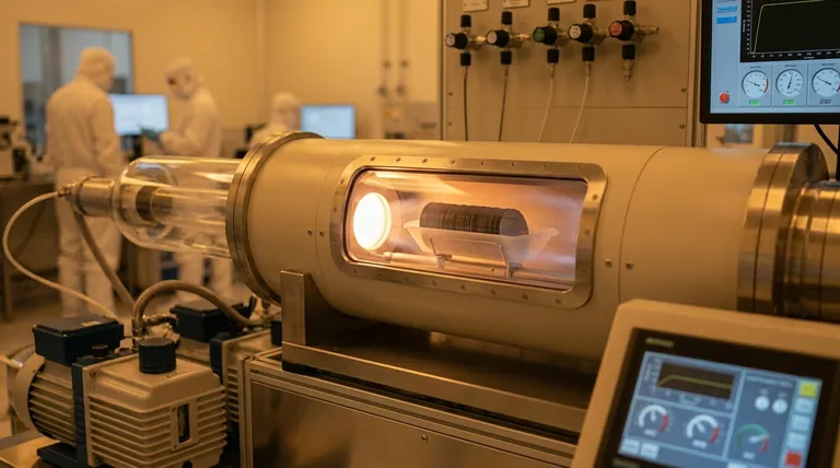
A Step-by-Step Look Inside an LPCVD Reactor
A typical LPCVD process occurs in a horizontal quartz tube furnace capable of holding a large batch of wafers, making it highly efficient.
1. Loading and Pump-Down
Wafers are loaded vertically into a quartz "boat," which is then pushed into the center of the furnace tube. The system is sealed and pumped down to its base pressure.
2. Temperature Ramp and Stabilization
The furnace heats the wafers to the precise process temperature. The system holds at this temperature to ensure every wafer in the batch is thermally stable and uniform.
3. Gas Introduction and Deposition
The precursor gases are introduced into the tube at a controlled flow rate. The chemical reaction begins on all hot surfaces, including the wafers, depositing a solid thin film.
4. Purge and Cool-Down
Once the desired film thickness is achieved, the precursor gas flow is stopped. The chamber is purged with an inert gas like nitrogen (N₂) to remove any reactive byproducts. The furnace then begins to cool.
5. Unloading
After cooling to a safe temperature, the system is vented back to atmospheric pressure, and the boat of freshly coated wafers is removed.
Understanding the Trade-offs and Limitations
While powerful, LPCVD is not the solution for every deposition need. Its primary limitation is a direct consequence of its greatest strength.
The High Thermal Budget
The most significant drawback is the high thermal budget—the combination of high temperature and long process time.
This heat can be problematic for devices with previously fabricated structures, such as low-melting-point metals (like aluminum) or precisely doped regions that could diffuse at high temperatures. This often restricts LPCVD to the earlier stages of device manufacturing.
Slower Deposition Rates
Compared to atmospheric pressure methods (APCVD), LPCVD is significantly slower. The priority is film quality and conformality, not raw speed.
Film Stress
High-temperature deposition can induce significant intrinsic stress in the film, which can cause issues like wafer bowing or film cracking if not properly managed through process optimization.
Making the Right Choice for Your Goal
Selecting a deposition technology requires matching the process capabilities to your specific goal and constraints.
- If your primary focus is coating complex 3D structures (like trenches or high-aspect-ratio features): LPCVD is the industry standard due to its unmatched conformality.
- If your primary focus is depositing films on temperature-sensitive substrates: The high thermal budget of LPCVD is a major liability; Plasma-Enhanced CVD (PECVD) is the superior choice.
- If your primary focus is high-throughput deposition of simple, non-conformal layers: LPCVD is often too slow and complex; a simpler method like APCVD may be more cost-effective.
By understanding these fundamental trade-offs, you can confidently determine when LPCVD is the right tool to achieve a high-quality, reliable thin film.
Summary Table:
| LPCVD Component | Key Function | Typical Parameters |
|---|---|---|
| Vacuum (Low Pressure) | Increases gas molecule mean free path for superior conformality | 10 - 1000 mTorr |
| High Temperature | Provides activation energy for surface chemical reactions | 500°C - 900°C |
| Precursor Gases | Supplies atoms for thin film formation (e.g., SiH₄, TEOS) | Controlled flow rates |
| Process Outcome | Exceptional step coverage and film uniformity | Batch processing for efficiency |
Need High-Quality Thin Films for Your Research or Production?
KINTEK specializes in providing advanced lab equipment and consumables for semiconductor and materials research. Our LPCVD systems and expertise help laboratories achieve precise, uniform thin film deposition with excellent conformality for complex structures.
Whether you're working on semiconductor devices, MEMS, or advanced coatings, KINTEK has the solutions to support your thin film deposition needs.
Contact our experts today to discuss how our LPCVD equipment and consumables can enhance your laboratory's capabilities and research outcomes.
Visual Guide

Related Products
- Chemical Vapor Deposition CVD Equipment System Chamber Slide PECVD Tube Furnace with Liquid Gasifier PECVD Machine
- Inclined Rotary Plasma Enhanced Chemical Vapor Deposition PECVD Equipment Tube Furnace Machine
- RF PECVD System Radio Frequency Plasma-Enhanced Chemical Vapor Deposition RF PECVD
- Microwave Plasma Chemical Vapor Deposition MPCVD Machine System Reactor for Lab and Diamond Growth
- 915MHz MPCVD Diamond Machine Microwave Plasma Chemical Vapor Deposition System Reactor
People Also Ask
- What are the advantages of chemical vapor deposition? Achieve Superior Thin Films for Your Lab
- What types of substrates are used in CVD to facilitate graphene films? Optimize Graphene Growth with the Right Catalyst
- How expensive is chemical vapor deposition? Understanding the True Cost of High-Performance Coating
- What happens during deposition chemistry? Building Thin Films from Gaseous Precursors
- Why is Chemical Vapor Deposition (CVD) equipment uniquely suited for constructing hierarchical superhydrophobic structures?


