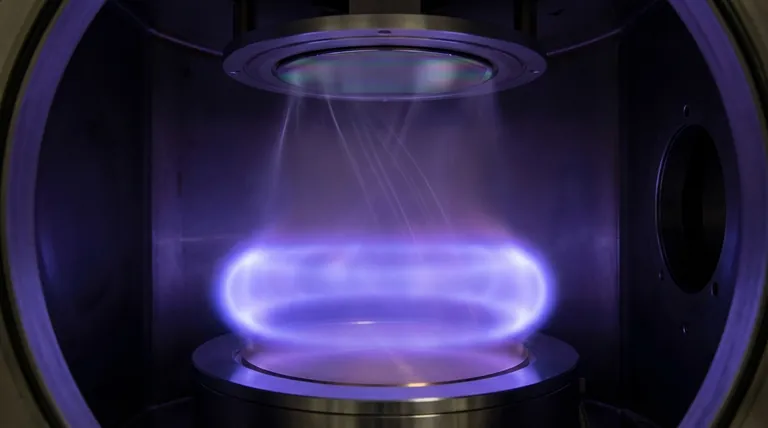
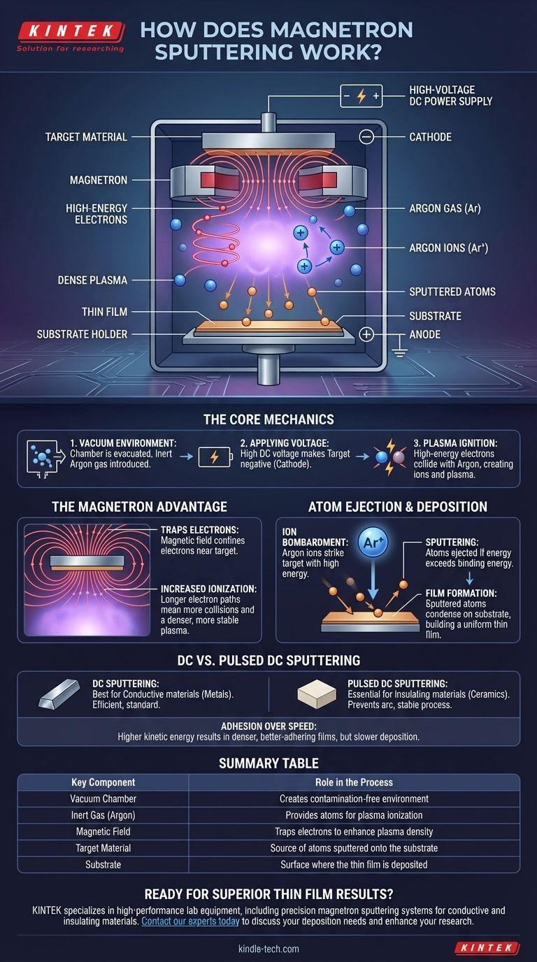
At its core, magnetron sputtering is a highly controlled physical vapor deposition (PVD) process that uses a magnetic field to enhance the creation of a plasma. This plasma bombards a source material, or "target," with ions, physically knocking atoms loose. These ejected atoms then travel through a vacuum and condense onto a substrate, building a thin, uniform film with exceptional precision.
The critical insight is not just about bombarding a target. The "magnetron" in the name refers to the strategic use of a magnetic field to trap electrons near the target, dramatically increasing the efficiency of plasma generation. This leads to a denser plasma, a faster deposition rate, and the ability to create higher-quality films at lower pressures.
The Core Mechanics of the Sputtering Process
To understand how magnetron sputtering works, it's best to break it down into a sequence of foundational steps that occur within a specialized vacuum chamber.
The Vacuum Environment
The entire process must take place in a vacuum chamber. This is crucial to remove any unwanted air or particles that could contaminate the final film.
Once a vacuum is established, a small, precisely controlled amount of an inert gas, most commonly Argon (Ar), is introduced. This gas provides the atoms that will be ionized to create the plasma.
Applying Voltage to Create Plasma
A high-voltage DC power supply is used to create a strong electric field. The material to be deposited, known as the target, is given a large negative charge (making it the cathode).
The substrate holder or the chamber walls typically act as the anode (positive or grounded). This voltage difference, often around -300V or more, is what energizes the system.
The Ignition of Plasma
The strong electric field accelerates free electrons in the chamber. These high-energy electrons collide with the neutral Argon atoms.
These collisions are forceful enough to knock electrons off the Argon atoms, creating positively charged Argon ions (Ar+) and more free electrons. This cascade of collisions ignites and sustains a glowing, ionized gas cloud known as a plasma.
The "Magnetron" Advantage: A More Efficient Plasma
Standard sputtering works, but it's inefficient. The addition of a magnetron—a configuration of powerful magnets placed behind the target—is what makes the process so effective.
The Role of the Magnetic Field
The magnetic field projects through the target and creates a confinement zone directly in front of its surface.
This magnetic field traps the lighter, negatively charged electrons, forcing them into a spiral path near the target instead of allowing them to escape.
Increased Ionization and Sputtering
Because the electrons are trapped, their path length is significantly increased, which dramatically raises the probability that they will collide with and ionize neutral Argon atoms.
This creates a much denser and more stable plasma concentrated right where it is needed most. The now-abundant positive Argon ions are strongly attracted to the negatively charged target.
Atom Ejection and Deposition
The Argon ions accelerate and bombard the target surface with immense kinetic energy.
If the energy transferred by an ion is greater than the surface binding energy of the target material, it physically knocks out, or "sputters," neutral atoms from the target. These sputtered atoms travel through the vacuum and land on the substrate, condensing to form the desired thin film.
Understanding the Trade-offs and Variations
While powerful, magnetron sputtering is a complex process with specific applications and limitations that require careful consideration.
DC vs. Pulsed DC Sputtering
Direct Current (DC) sputtering is the standard method and works exceptionally well for electrically conductive target materials, like most metals.
For insulating (dielectric) materials like ceramics, a charge can build up on the target surface, deflecting ions and leading to arcing. Pulsed DC sputtering solves this by periodically reversing the voltage for a short time to neutralize this charge buildup, allowing for stable deposition.
The Importance of Process Control
The quality of the resulting film—its density, adhesion, grain structure, and electrical properties—is not automatic. It depends on meticulous control over variables like gas pressure, voltage, magnetic field strength, and substrate temperature.
Adhesion Over Speed
The sputtered atoms arrive at the substrate with significantly more kinetic energy compared to other methods like thermal evaporation. This results in denser, more uniform, and better-adhering films. The trade-off is that sputtering is often a slower deposition process.
Making the Right Choice for Your Goal
Selecting the right sputtering technique is entirely dependent on the material you are working with and the desired properties of the final film.
- If your primary focus is depositing a conductive metal film: Standard DC Magnetron Sputtering is the efficient, reliable, and industry-standard choice.
- If your primary focus is depositing an insulating ceramic or oxide: Pulsed DC Sputtering is essential to prevent charge buildup and ensure a stable, arc-free process.
- If your primary focus is achieving maximum film density and adhesion: Magnetron sputtering is superior to many other deposition techniques due to the higher energy of the depositing particles.
Ultimately, magnetron sputtering provides an indispensable level of control for creating the high-performance thin films that are foundational to modern electronics, optics, and materials science.
Summary Table:
| Key Component | Role in the Process |
|---|---|
| Vacuum Chamber | Creates a contamination-free environment |
| Inert Gas (Argon) | Provides atoms for plasma ionization |
| Magnetic Field | Traps electrons to enhance plasma density |
| Target Material | Source of atoms sputtered onto the substrate |
| Substrate | Surface where the thin film is deposited |
Ready to achieve superior thin film results in your lab?
KINTEK specializes in high-performance lab equipment, including magnetron sputtering systems designed for precision and reliability. Whether you're working with conductive metals or insulating ceramics, our solutions help you create dense, uniform films with excellent adhesion.
Contact our experts today to discuss your specific deposition needs and discover how KINTEK can enhance your research and production processes.
Visual Guide
Related Products
- Spark Plasma Sintering Furnace SPS Furnace
- RF PECVD System Radio Frequency Plasma-Enhanced Chemical Vapor Deposition RF PECVD
People Also Ask
- What is the mechanism of SPS process? A Deep Dive into Rapid, Low-Temperature Sintering
- What is the theory of spark plasma sintering? A Guide to Rapid, Low-Temperature Densification
- What are the fundamentals of spark plasma sintering process? Unlock Rapid, High-Performance Material Consolidation
- What is the process fundamentals of spark plasma sintering? Achieve Rapid, High-Density Material Consolidation
- What technical advantages does a Spark Plasma Sintering (SPS) furnace offer for LZP ceramics? Enhance Ionic Conductivity

