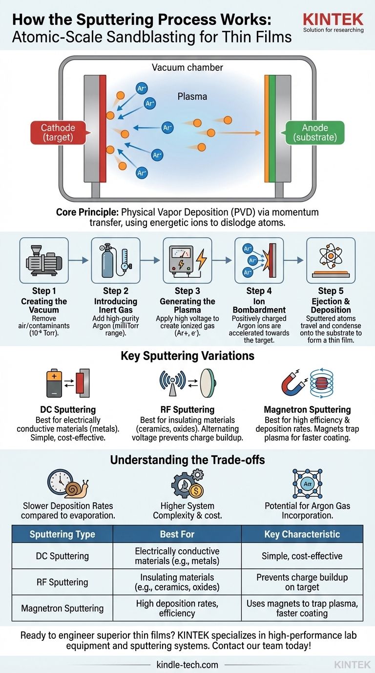
At its core, the sputtering process is a physical vapor deposition (PVD) method that works like an atomic-scale sandblaster. Inside a vacuum chamber, high-energy ions are accelerated to bombard a source material, called the target. This collision has enough force to physically knock atoms off the target's surface, which then travel through the vacuum and deposit onto a substrate, building a thin, uniform film layer by layer.
Sputtering is not a chemical reaction but a physical process of momentum transfer. Its power lies in using energetic ions to dislodge atoms from virtually any material, allowing for the creation of high-quality, strongly bonded thin films on a substrate, even from materials with extremely high melting points.

The Foundational Steps of Sputtering
The sputtering process is a precisely controlled sequence designed to create a pure, energetic environment for film growth. Each step serves a critical function in achieving a high-quality coating.
Step 1: Creating the Vacuum
The entire process occurs within a sealed chamber that is first pumped down to a high vacuum, typically around 10⁻⁶ Torr or lower.
This initial vacuum is crucial for removing air and other contaminant molecules like water vapor. Without it, these impurities would get incorporated into the film, degrading its quality, or react with the sputtered atoms mid-flight.
Step 2: Introducing an Inert Gas
Once the base vacuum is achieved, a high-purity inert gas—most commonly Argon (Ar)—is introduced into the chamber.
The chamber pressure is carefully raised and stabilized to a working pressure in the milliTorr range. Argon is used because it is chemically non-reactive, relatively heavy, and ionizes efficiently without reacting with the target or substrate.
Step 3: Generating the Plasma
A high voltage is applied between two electrodes inside the chamber. The source material (the target) is configured as the cathode (negative electrode).
This strong electric field energizes the argon gas, stripping electrons from the argon atoms and creating a visible glow known as a plasma. This plasma is a charged soup of positive argon ions (Ar+) and free electrons.
Step 4: Ion Bombardment
The positively charged argon ions (Ar+) are powerfully accelerated by the electric field and drawn toward the negatively charged target.
They collide with the target surface with significant kinetic energy. Think of these ions as atomic cannonballs.
Step 5: Ejection and Deposition
The impact of an argon ion transfers enough momentum to atoms on the target's surface to overcome their binding forces, causing them to be ejected or "sputtered."
These newly freed atoms travel in a straight line through the low-pressure argon environment until they strike the substrate (the part being coated). There, they condense and build up, forming a dense and highly adherent thin film.
Key Sputtering Variations for Different Needs
While the basic principle remains the same, different sputtering techniques have been developed to handle various materials and improve efficiency.
DC Sputtering: The Basic Model
Direct Current (DC) sputtering uses a constant negative voltage on the target. It is simple, effective, and widely used.
However, it only works for electrically conductive target materials, like metals. Insulating materials would quickly build up a positive charge from the ion bombardment, effectively neutralizing the electric field and stopping the process.
RF Sputtering: For Insulating Materials
Radio Frequency (RF) sputtering solves the problem of coating with non-conductive materials like ceramics or oxides.
Instead of a constant DC voltage, it uses an alternating high-frequency voltage (typically 13.56 MHz). This rapid switching of polarity prevents charge from building up on the target surface, allowing the sputtering of any material, regardless of its electrical properties.
Magnetron Sputtering: For Higher Efficiency
Magnetron sputtering is the most common industrial method because it dramatically increases deposition speed.
Powerful magnets are placed behind the target to create a magnetic field that traps the free electrons from the plasma directly in front of the target's surface. These trapped electrons fly in a spiral path, significantly increasing their chances of colliding with and ionizing argon atoms. This creates a much denser plasma, leading to more ion bombardment and a faster sputtering rate.
Understanding the Trade-offs
Sputtering is a powerful and versatile technique, but it is essential to understand its practical limitations compared to other methods.
Slower Deposition Rates
Compared to some forms of thermal evaporation, sputtering can be a slower process. The atom-by-atom ejection is inherently less rapid than boiling a material in a crucible. While magnetron sputtering helps, high-rate evaporation can still be faster for certain applications.
Higher System Complexity
Sputtering systems are more complex and expensive than simple thermal evaporators. They require high-voltage power supplies (DC or RF), precise gas flow controllers, and robust vacuum systems, increasing both the initial investment and maintenance overhead.
Potential for Gas Incorporation
Because the process occurs in an argon environment, a small percentage of argon atoms can become embedded within the growing film. For most applications, this is negligible, but for highly sensitive optical or electronic films, it can be a factor that influences material properties.
Making the Right Choice for Your Goal
Selecting the correct sputtering technique is a direct function of your target material and your desired process efficiency.
- If your primary focus is coating a conductive material like a metal: Standard DC sputtering is the most straightforward and cost-effective method.
- If your primary focus is coating an insulating material like a ceramic (Al₂O₃) or quartz (SiO₂): RF sputtering is the necessary choice to overcome charge accumulation on the target.
- If your primary focus is achieving high deposition rates and minimizing substrate heating: Magnetron sputtering, whether DC for metals or RF for insulators, is the industry standard for efficient production.
By understanding these core principles, you can precisely control the deposition of materials to engineer thin films with specific, desired properties at the atomic level.
Summary Table:
| Sputtering Type | Best For | Key Characteristic |
|---|---|---|
| DC Sputtering | Electrically conductive materials (e.g., metals) | Simple, cost-effective |
| RF Sputtering | Insulating materials (e.g., ceramics, oxides) | Prevents charge buildup on target |
| Magnetron Sputtering | High deposition rates, efficiency | Uses magnets to trap plasma, faster coating |
Ready to engineer superior thin films? The right sputtering equipment is critical for your R&D or production success. KINTEK specializes in high-performance lab equipment, including sputtering systems, to meet your specific material deposition needs. Our experts can help you select the perfect configuration for conductive or insulating targets. Contact our team today to discuss how we can enhance your laboratory's capabilities!
Visual Guide
Related Products
- Spark Plasma Sintering Furnace SPS Furnace
- Vacuum Induction Melting Spinning System Arc Melting Furnace
- Chemical Vapor Deposition CVD Equipment System Chamber Slide PECVD Tube Furnace with Liquid Gasifier PECVD Machine
- Customer Made Versatile CVD Tube Furnace Chemical Vapor Deposition Chamber System Equipment
People Also Ask
- What is the mechanism of SPS process? A Deep Dive into Rapid, Low-Temperature Sintering
- What is SPS sintering method? A Guide to High-Speed, High-Performance Material Fabrication
- What is the difference between spark plasma sintering and flash sintering? A Guide to Advanced Sintering Methods
- What is the process fundamentals of spark plasma sintering? Achieve Rapid, High-Density Material Consolidation
- What is the pressure for spark plasma sintering? A Guide to Optimizing SPS Parameters


