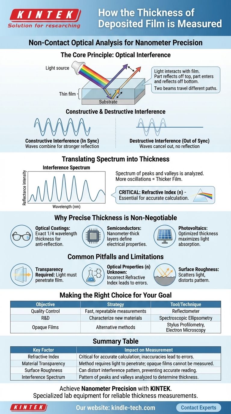
In material science and engineering, the most common non-contact method for measuring the thickness of a deposited film is through optical analysis. This technique uses light to analyze the interference pattern created by reflections from both the top and bottom surfaces of the film. By measuring this pattern, typically in the nanometer range, a precise thickness can be calculated.
The core principle is simple: by analyzing how light waves interfere after bouncing off a film's top and bottom boundaries, we can determine its thickness. However, the accuracy of this measurement is critically dependent on knowing the material's refractive index.
The Core Principle: Optical Interference
Understanding how thin film thickness is measured begins with understanding how light behaves when it encounters a semi-transparent layer.
How Light Interacts with a Thin Film
When a beam of light strikes a thin film, a portion of it reflects off the top surface. The rest of the light enters the film, travels through it, and then reflects off the bottom surface (the interface with the substrate).
This creates two separate beams of reflected light traveling back toward the observer or detector. The second beam has traveled a longer path than the first.
Constructive and Destructive Interference
Because one light beam has traveled farther, its waves may be in or out of sync with the waves from the first beam.
When the waves are perfectly in sync, they combine to create a stronger reflection (constructive interference). When they are out of sync, they cancel each other out (destructive interference).
Translating an Interference Spectrum into Thickness
A measurement tool shines light of many wavelengths (colors) onto the film and records the intensity of the reflection for each one. This creates an interference spectrum—a unique pattern of peaks and valleys.
The number of peaks and valleys over a given range of wavelengths is directly proportional to the thickness of the film. A thicker film creates a longer path difference, resulting in more oscillations in the spectrum.
The Critical Role of Refractive Index
The refractive index of the film's material is a crucial variable. It describes how much the speed of light slows down upon entering the material.
Without an accurate refractive index value, the calculation converting the interference spectrum into a physical thickness will be incorrect. The system must know how fast light was traveling through the film to know what path distance the interference pattern represents.
Why Precise Thickness is Non-Negotiable
In advanced applications, controlling film thickness is not just a matter of quality; it dictates the fundamental function of the final product.
Functionality in Optical Coatings
The anti-reflection coating on eyeglasses or camera lenses must have a thickness that is precisely one-quarter of the wavelength of light it's designed to cancel out. Any deviation renders the coating ineffective.
Performance in Semiconductors
In semiconductor manufacturing, layers of material deposited onto a silicon wafer are mere nanometers thick. The electrical properties and performance of the final microchip are entirely dependent on these layers being the exact specified thickness.
Efficiency in Photovoltaics
The layers in a solar cell are engineered to absorb specific wavelengths of light. The thickness of each layer is optimized to maximize light absorption and, therefore, the cell's energy conversion efficiency.
Common Pitfalls and Limitations
While powerful, the optical interference method has specific requirements that must be met for an accurate measurement.
Material Transparency is Required
This method fundamentally relies on light passing through the film to reflect off the bottom interface. If the film is completely opaque to the light being used, no measurement can be made.
Knowledge of Optical Properties is Essential
As mentioned, an unknown or incorrect refractive index is the most common source of error. If the deposition process changes the material's density or composition, its refractive index may change, requiring re-characterization.
Surface Roughness Can Interfere
The model assumes smooth, parallel surfaces. If the top surface of the film is very rough, it can scatter light unpredictably instead of reflecting it cleanly, which can distort or destroy the interference pattern and prevent an accurate reading.
Making the Right Choice for Your Goal
To apply this principle effectively, you must align your measurement strategy with your objective.
- If your primary focus is quality control in manufacturing: The key is to use a reflectometer for fast, repeatable, and non-destructive measurements, ensuring process consistency.
- If your primary focus is research and development: You need to precisely characterize new materials, often using advanced spectroscopic ellipsometry to determine both thickness and refractive index simultaneously.
- If you are working with opaque metal films: You must recognize that optical methods are unsuitable and investigate alternative techniques like stylus profilometry or electron microscopy.
Ultimately, precise measurement is the foundation of control, enabling the creation of advanced materials that function exactly as designed.
Summary Table:
| Key Factor | Impact on Measurement |
|---|---|
| Refractive Index | Critical for accurate calculation; inaccuracies lead to errors. |
| Material Transparency | Method requires light to penetrate the film; opaque films cannot be measured. |
| Surface Roughness | Can distort the interference pattern, preventing an accurate reading. |
| Interference Spectrum | The pattern of peaks and valleys is directly analyzed to determine thickness. |
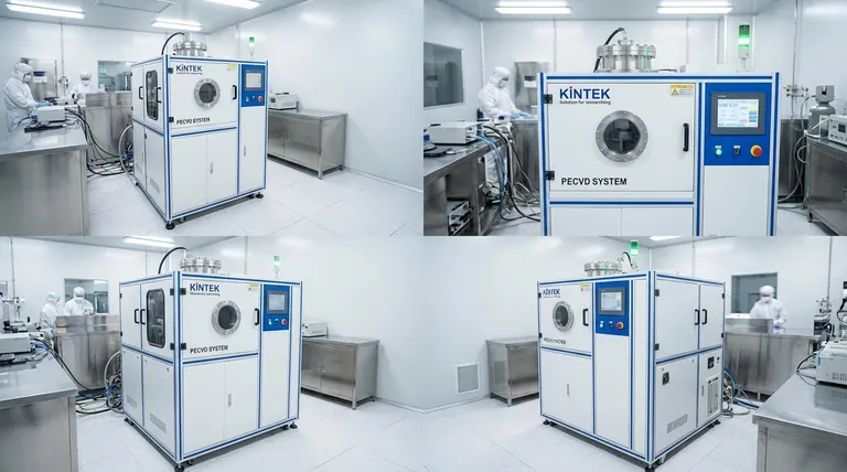
Achieve Nanometer Precision in Your Lab
Accurate film thickness is non-negotiable for the functionality of semiconductors, optical coatings, and photovoltaics. Whether your focus is on R&D or quality control, having the right equipment is paramount.
KINTEK specializes in providing high-precision lab equipment, including reflectometers and ellipsometers, designed to deliver reliable thickness measurements for your specific materials and applications. Our expertise ensures you can control your deposition process with confidence.
Ready to enhance your measurement capabilities? Contact our experts today via our Contact Form to discuss your specific needs and discover how KINTEK's solutions can bring precision and reliability to your laboratory.
Visual Guide
Related Products
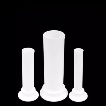
- Custom PTFE Teflon Parts Manufacturer for PTFE Measuring Cylinder 10/50/100ml
- Electron Beam Evaporation Coating Oxygen-Free Copper Crucible and Evaporation Boat
- Small Lab Rubber Calendering Machine
- Lab Blown Film Extrusion Three Layer Co-Extrusion Film Blowing Machine
- Customizable XRD Sample Holders for Diverse Research Applications
People Also Ask
- What are the disadvantages of flash pyrolysis oil? Overcoming Key Challenges in Bio-Oil Utilization
- What is the best solvent for FTIR? Master Solvent Selection for Clear, Accurate Spectra
- Why is a capacitance manometer preferred for RF plasma systems? Ensure Precise Gas-Independent Pressure Monitoring
- What role do standard pyrometric cones (PCE Cones) play during refractoriness testing? Ensure High-Temp Stability
- What are the contaminants in plastic pyrolysis oil? Manage Impurities for Commercial Success