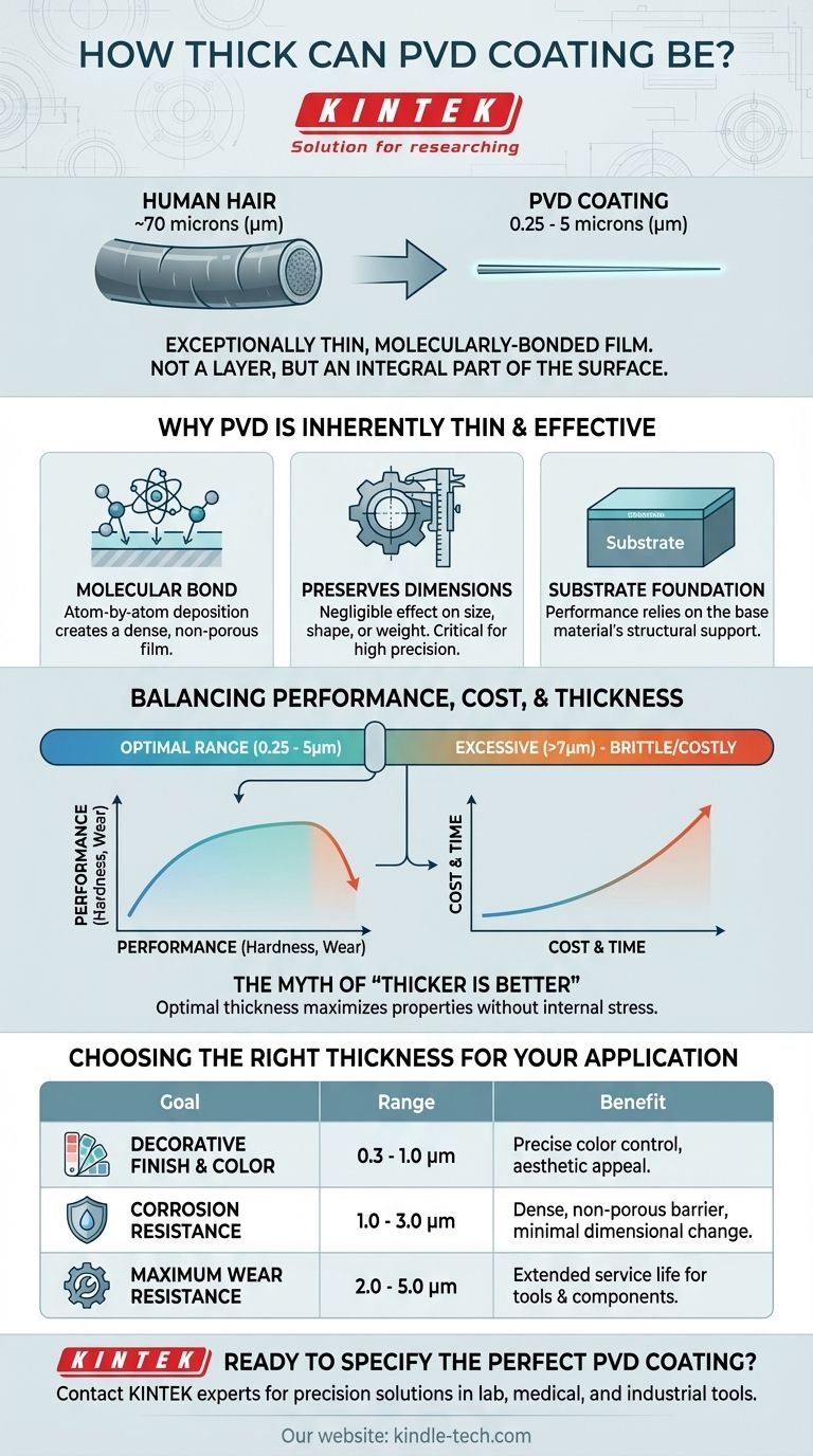
In practice, a Physical Vapor Deposition (PVD) coating is exceptionally thin, with a typical thickness ranging from 0.25 to 5 microns (micrometers). To put this in perspective, a human hair is about 70 microns thick, meaning even the thickest standard PVD coatings are more than ten times thinner. This thinness is not a limitation but a fundamental feature of the technology, designed to enhance a material's properties without altering its physical dimensions.
The goal of PVD is not to add a thick, protective shell, but to create a thin, molecularly-bonded film. The specific thickness is precisely engineered to optimize properties like hardness, wear resistance, and color, making the concept of "thicker is better" a common and costly misunderstanding.
Why PVD Coatings Are Inherently Thin
PVD is a sophisticated vacuum deposition process, fundamentally different from conventional methods like painting or electroplating. This distinction is key to understanding the nature of its thickness.
A Molecular Bond, Not a Layer of Paint
PVD application techniques—such as sputtering or thermal evaporation—deposit material atom by atom onto a substrate's surface. This creates a strong, molecular-level bond.
The result is a dense, non-porous film that becomes an integral part of the surface itself, rather than a distinct layer sitting on top of it.
Preserving Dimensional Tolerance
Because the coating is measured in single-digit microns, it has a negligible effect on a component's size, shape, or weight.
This is critical for high-precision applications like cutting tools, medical implants, or aerospace components, where even minute changes in dimension can lead to failure.
The Substrate Provides the Foundation
A PVD coating’s performance is a direct partnership with the material underneath it, known as the substrate. The coating provides extreme surface hardness, but the substrate provides the structural support.
Applying a hard PVD coating to a soft substrate is like laying a thin sheet of glass on a mattress—it will flex and crack under pressure. Therefore, the properties of the base material are just as important as the coating itself.
How Thickness Impacts Performance
While the range is narrow, varying the thickness within the 0.25 to 5-micron window allows engineers to fine-tune the coating for specific outcomes.
Hardness and Wear Resistance
For applications requiring high durability, such as on industrial tools, a thicker coating (typically 2 to 5 microns) can provide a longer wear life. The added material provides a greater buffer against abrasive forces.
Corrosion Resistance
The exceptional corrosion resistance of PVD comes from the density and chemical inertness of the film, not its bulk. Even a thin coating of 1 to 2 microns can create a complete barrier that prevents oxidation and chemical attack.
Color and Aesthetics
In decorative applications, thickness has a direct impact on color. The perceived color of many PVD coatings is the result of light interference, similar to the rainbow sheen on a soap bubble.
Precise control over thickness, often down to a few nanometers, is required to achieve a specific, consistent color across a product.
Understanding the Trade-offs
Specifying the correct thickness is a critical engineering decision that involves balancing competing factors. Simply asking for the "thickest possible" coating is almost always the wrong approach.
The Myth of "Thicker is Better"
As PVD coatings get thicker, they accumulate internal stress. An excessively thick coating (e.g., beyond 7-10 microns) can become brittle and prone to chipping, cracking, or delaminating from the surface.
The optimal thickness is one that maximizes performance without introducing this internal stress, ensuring the coating remains adhered and intact.
Balancing Performance and Cost
PVD is a time-based process. A thicker coating requires a longer cycle time inside the vacuum chamber, which directly increases the cost of the operation.
The goal is always to specify the minimum effective thickness that meets the application's performance requirements, thus optimizing both function and cost.
Choosing the Right Thickness for Your Application
The ideal specification depends entirely on your primary goal. Use the following as a guide for discussing your project with a coating expert.
- If your primary focus is a decorative finish and color consistency: A thinner, highly controlled coating (e.g., 0.3-1.0 microns) is typically specified to achieve the desired optical effects.
- If your primary focus is maximum wear resistance for tools or heavy-use components: A thicker coating in the optimal range (e.g., 2.0-5.0 microns) provides a more substantial wear surface.
- If your primary focus is corrosion resistance with minimal dimensional change: A standard, mid-range thickness (e.g., 1.0-3.0 microns) offers a robust and non-porous barrier ideal for most environments.
Ultimately, the ideal PVD coating thickness is an engineered specification, not a simple measure of quality.
Summary Table:
| Application Goal | Typical Thickness Range | Key Benefit |
|---|---|---|
| Decorative Finish & Color | 0.3 - 1.0 microns | Precise color control, aesthetic appeal |
| Corrosion Resistance | 1.0 - 3.0 microns | Dense, non-porous barrier, minimal dimensional change |
| Maximum Wear Resistance | 2.0 - 5.0 microns | Extended service life for tools and components |
Ready to specify the perfect PVD coating for your application?
Choosing the right thickness is critical for performance and cost-efficiency. The experts at KINTEK specialize in precision PVD coatings for laboratory equipment, medical devices, and industrial tools. We'll help you determine the minimum effective thickness to achieve superior hardness, corrosion resistance, and color consistency.
Contact KINTEK today to discuss your project and get a tailored solution that maximizes the value of your components.
Visual Guide
Related Products
- RF PECVD System Radio Frequency Plasma-Enhanced Chemical Vapor Deposition RF PECVD
- Chemical Vapor Deposition CVD Equipment System Chamber Slide PECVD Tube Furnace with Liquid Gasifier PECVD Machine
- Split Chamber CVD Tube Furnace with Vacuum Station Chemical Vapor Deposition System Equipment Machine
- Molybdenum Tungsten Tantalum Special Shape Evaporation Boat
- VHP Sterilization Equipment Hydrogen Peroxide H2O2 Space Sterilizer
People Also Ask
- What is an example of PECVD? RF-PECVD for High-Quality Thin Film Deposition
- Why is PECVD environment friendly? Understanding the Eco-Friendly Benefits of Plasma-Enhanced Coating
- What are the advantages of PECVD? Enable Low-Temperature, High-Quality Thin-Film Deposition
- How does RF power create plasma? Achieve Stable, High-Density Plasma for Your Applications
- What are the applications of PECVD? Essential for Semiconductors, MEMS, and Solar Cells

