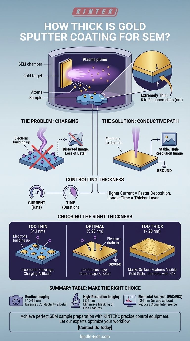
Typically, gold sputter coating for SEM is extremely thin, ranging from 5 to 20 nanometers (nm). This thickness is not a random value; it is a highly controlled parameter critical for achieving a clear image. The goal is to deposit just enough conductive material to prevent electron charging without obscuring the microscopic surface details of the sample being analyzed.
The thickness of a gold sputter coat is a fundamental trade-off. It must be thick enough to create a continuous conductive layer that prevents image distortion, but thin enough so that the coating itself does not hide the true surface topography of your sample.
Why Sputter Coating is Necessary for SEM
To understand the importance of thickness, you must first understand the problem sputter coating solves in Scanning Electron Microscopy (SEM).
The Problem of "Charging"
SEMs work by bombarding a sample with a focused beam of electrons. If the sample is not electrically conductive, these electrons accumulate on the surface, an effect known as "charging." This buildup of negative charge deflects the incoming electron beam, leading to bright patches, distorted images, and a complete loss of surface detail.
The Solution: A Conductive Path
A thin layer of a conductive metal, like gold, provides a path for these excess electrons to drain away to the instrument's ground. This neutralizes the sample surface, allowing the electron beam to interact with it cleanly and produce a stable, high-resolution image.
How Sputter Coating Thickness is Controlled
The references you provided correctly describe the core mechanism of sputter coating: using a plasma in a vacuum to eject gold atoms from a target onto your sample. The thickness of this deposited layer is determined by a few key variables.
The Role of Plasma and Current
In the sputter coater, an electric field accelerates argon ions into a gold target, dislodging gold atoms. The current setting on the coater controls the rate of this process—a higher current ejects more gold atoms per second.
The Importance of Time
The most direct control you have is the coating time. For a given current, the longer you run the process, the more gold atoms will land on your sample, and the thicker the resulting layer will be. Modern coaters often have built-in thickness monitors for precise control.
Understanding the Trade-offs
Choosing the right thickness is an exercise in balancing competing requirements. There is no single "perfect" thickness for every application.
Too Thin: Incomplete Coverage
If the gold layer is too thin (e.g., below 2-3 nm), it may not form a continuous film. Instead, you get isolated "islands" of gold. This results in incomplete charge dissipation and can still produce charging artifacts in your image, defeating the purpose of coating.
Too Thick: Obscuring Surface Features
If the gold layer is too thick (e.g., over 20-30 nm), it begins to mask the sample's authentic surface. You are no longer imaging your sample's topography but rather the topography of the gold coating itself. The inherent grain structure of the sputtered gold can become visible, limiting the ultimate resolution you can achieve.
Interference with Elemental Analysis
For techniques like Energy-Dispersive X-ray Spectroscopy (EDS/EDX), a thick gold coat is highly problematic. The gold layer can absorb X-rays emitted from lighter elements in your sample or generate its own X-ray signals (the "M-line" for gold), interfering with accurate elemental analysis.
Making the Right Choice for Your Goal
Select your coating thickness based on your primary analytical objective.
- If your primary focus is routine, low-to-mid magnification imaging: A standard 10-15 nm coating is a reliable choice that provides excellent conductivity for most non-conductive samples.
- If your primary focus is high-resolution imaging of fine surface details: Aim for the thinnest possible continuous layer, typically between 3-5 nm, to minimize any masking effects from the coating itself.
- If your primary focus is elemental analysis (EDS/EDX): Use the thinnest possible gold layer (2-5 nm) to reduce signal absorption, or strongly consider using a carbon coater instead, as carbon's low atomic number creates far less interference.
Ultimately, controlling coating thickness is about ensuring the data you collect reflects the reality of your sample, not the artifacts of the preparation process.
Summary Table:
| Coating Goal | Recommended Thickness | Key Consideration |
|---|---|---|
| Routine Imaging | 10-15 nm | Balances conductivity and detail preservation |
| High-Resolution Imaging | 3-5 nm | Minimizes coating masking of fine features |
| Elemental Analysis (EDS/EDX) | 2-5 nm (or use carbon) | Reduces interference with X-ray signals |
Achieve perfect SEM sample preparation with KINTEK.
Choosing the right sputter coating thickness is critical for obtaining accurate, high-quality images and elemental data. Our lab equipment and consumables are designed to give you precise control over this process, ensuring your samples are prepared correctly for your specific analytical goals.
Let our experts help you optimize your workflow. Contact us today to discuss your laboratory needs and discover how KINTEK's solutions can enhance your research and analysis.
Visual Guide
Related Products
- Custom CVD Diamond Coating for Lab Applications
- Electron Beam Evaporation Coating Oxygen-Free Copper Crucible and Evaporation Boat
- RF PECVD System Radio Frequency Plasma-Enhanced Chemical Vapor Deposition RF PECVD
- Aluminized Ceramic Evaporation Boat for Thin Film Deposition
- Vacuum Hot Press Furnace Machine for Lamination and Heating
People Also Ask
- How thick is CVD diamond coating? Balancing Durability and Stress for Optimal Performance
- How long does diamond coating last? Maximize Lifespan with the Right Coating for Your Application
- What are the three types of coating? A Guide to Architectural, Industrial, and Special Purpose
- What are diamond coated films? Enhance Materials with Super-Hard, Transparent Layers
- Is diamond coating worth it? Maximize Component Life and Performance