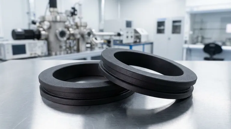
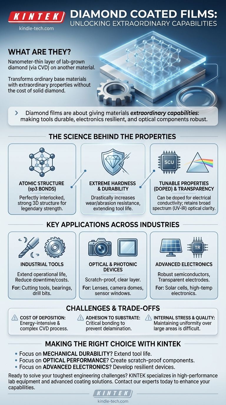
At its core, a diamond coated film is an extremely thin layer of lab-grown diamond, often just nanometers thick, that is deposited onto the surface of another material. This process transfers diamond's exceptional properties—like extreme hardness and optical clarity—to a base material, such as a metal tool or a glass lens, without the cost or constraints of using solid diamond.
Diamond films are not about making things out of diamond, but about giving ordinary materials extraordinary capabilities. By applying a microscopic layer of diamond, we can make tools dramatically more durable, electronics more resilient, and optical components more robust.
The Science Behind the Superior Properties
To understand the value of diamond films, we must first understand the fundamental properties of diamond itself. These films are synthesized in labs, typically through a process called Chemical Vapor Deposition (CVD), which allows for precise control over the film's thickness and quality.
The Foundation: Atomic Structure
Diamond's legendary strength comes from its atomic structure. It consists of carbon atoms arranged in a crystal lattice where each atom is bonded to four others with incredibly strong covalent bonds (sp3 hybridization). This creates a perfectly interlocked, rigid 3D structure.
Extreme Hardness and Durability
This tight atomic lattice makes diamond the hardest known natural material. When applied as a film, this property is transferred to the surface of a tool, drastically increasing its resistance to wear and abrasion. This directly translates to longer tool life and improved efficiency in cutting and machining operations.
Tunable Electrical Conductivity
While pure diamond is an excellent electrical insulator, diamond films can be "doped" with elements like boron during the manufacturing process. This transforms the film into a semiconductor. This tunable conductivity is a key reason for its use in advanced electronics.
High Optical Transparency
High-quality diamond is transparent across a very broad spectrum of light, from ultraviolet (UV) to infrared (IR). Diamond films retain this property, making them ideal for protective coatings on optical components that must allow light to pass through without distortion.
Key Applications: From Industrial Tools to High-Tech Optics
The unique combination of these properties has unlocked applications across multiple industries. The choice of diamond film is always driven by the problem you are trying to solve.
Mechanical and Industrial Uses
The most common application leverages diamond's hardness. Coating cutting tools, drill bits, and industrial bearings with a nanometer-thin diamond film can extend their operational life by orders of magnitude, reducing downtime and replacement costs.
Optical and Photonic Devices
For optics, the combination of hardness and transparency is critical. Diamond films act as a perfectly clear, scratch-proof layer on lenses, camera domes, and sensor windows, protecting sensitive and expensive components from harsh environments.
Advanced Electronics
The semiconducting properties of doped diamond films make them promising for next-generation electronics. They can be used to create transparent electrodes for solar cells and displays, or robust transistors that can function at temperatures and radiation levels that would destroy traditional silicon components.
Understanding the Trade-offs and Challenges
Despite their remarkable advantages, diamond films are not a universal solution. Their adoption is governed by practical engineering and economic trade-offs.
The Cost of Deposition
Creating high-quality diamond films via CVD is an energy-intensive and technically complex process. This makes it significantly more expensive than many other hardening or coating techniques, restricting its use to high-value applications where the performance benefits justify the cost.
Adhesion to the Substrate
The bond between the diamond film and the underlying material (the substrate) is critical. If adhesion is poor, the film can delaminate or flake off under stress, rendering it useless. A great deal of research is focused on improving this interfacial bonding.
Internal Stress and Quality
Growing a perfectly uniform diamond film is challenging. Internal stresses can build up during the deposition process, which can impact the film's mechanical integrity and performance. Maintaining consistent quality over large surface areas remains a key manufacturing hurdle.
Making the Right Choice for Your Goal
Evaluating diamond films requires matching their unique strengths to your specific application. The decision to use this advanced material should be based on a clear performance requirement.
- If your primary focus is mechanical durability: Use diamond films to drastically extend the life of cutting tools and wear parts, reducing downtime and replacement costs.
- If your primary focus is optical performance: Leverage the film's transparency and toughness to create scratch-proof lenses, robust sensor windows, or more efficient solar cells.
- If your primary focus is advanced electronics: Explore doped diamond films for creating resilient, transparent electrodes or semiconductors that can operate in extreme temperature or radiation environments.
By understanding these distinct advantages, you can strategically apply this remarkable material to solve engineering challenges that were previously out of reach.
Summary Table:
| Property | Benefit | Key Application |
|---|---|---|
| Extreme Hardness | Drastically increases wear resistance | Cutting tools, industrial bearings |
| Broad Optical Transparency | Scratch-proof, clear from UV to IR | Lenses, sensor windows, camera domes |
| Tunable Electrical Conductivity | Enables robust semiconductors & electrodes | High-temperature electronics, solar cells |
Ready to solve your toughest engineering challenges with diamond coated films? KINTEK specializes in high-performance lab equipment and consumables, including advanced coating solutions. Our expertise can help you integrate diamond films to extend tool life, protect optical components, or develop next-generation electronics. Contact our experts today to discuss how we can enhance your laboratory's capabilities and drive your projects forward.
Visual Guide
Related Products
- Custom CVD Diamond Coating for Lab Applications
- Laboratory CVD Boron Doped Diamond Materials
- HFCVD Machine System Equipment for Drawing Die Nano-Diamond Coating
- CVD Diamond Domes for Industrial and Scientific Applications
- CVD Diamond Optical Windows for Lab Applications
People Also Ask
- What are the advantages of CVD coating? Superior Hardness and Uniformity for Demanding Applications
- What is CVD coating used for? Hardening Tools & Building Semiconductors for Industry
- How thick is CVD diamond coating? Balancing Durability and Stress for Optimal Performance
- What is CVD coating? Transform Your Material's Surface for Maximum Performance
- What is CVD diamond coating? Grow a Super-Hard, High-Performance Diamond Layer


