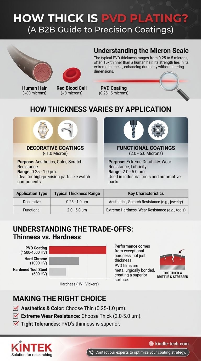
In short, the typical thickness of a Physical Vapor Deposition (PVD) coating ranges from 0.25 to 5 microns (micrometers). This range varies significantly based on the intended application, with decorative finishes being on the thinner end and functional, wear-resistant coatings on the thicker end. The coating is applied in a vacuum and forms a molecular bond with the substrate material.
The extreme thinness of PVD is its greatest strength. It creates a new, exceptionally hard surface that enhances an object's durability without altering its critical dimensions, texture, or weight in any meaningful way.

Understanding the Scale of a PVD Coating
To grasp the implications of PVD thickness, it's crucial to understand just how small a micron is. A single micron is one-millionth of a meter.
Putting "Microns" in Perspective
For comparison, a single red blood cell is about 8 microns in diameter. A human hair is approximately 80 microns thick.
This means that even a thick, 5-micron functional PVD coating is still more than 15 times thinner than a single strand of your hair.
A Feature, Not a Limitation
The thinness of a PVD coating is a key engineering advantage. Unlike thicker methods like electroplating or painting, PVD does not change a part's final dimensions, fit, or surface texture.
A component with a brushed finish will still have a brushed finish after PVD, and a high-polish part will remain a high-polish part. This is critical for high-precision components like watch parts, engine components, or surgical tools where even minute changes in tolerance can cause failure.
How Thickness Varies by Application
The specified thickness of a PVD coating is determined entirely by its purpose. There is no single "best" thickness; it is always a function of the desired outcome.
Decorative Coatings (Typically < 1.0 Micron)
For applications where the primary goal is color and improved scratch resistance—such as on faucets, watches, or jewelry—a thinner coating is ideal.
These coatings often range from 0.25 to 1.0 microns. This is more than sufficient to provide a durable, vibrant finish that resists tarnishing and everyday wear.
Functional Coatings (Typically 2.0 to 5.0 Microns)
For industrial applications where maximum durability is the priority, thicker coatings are used. This includes cutting tools, drill bits, firearm components, and automotive engine parts.
These functional coatings, typically 2.0 to 5.0 microns thick, are designed for extreme hardness and lubricity, extending the life of tools and components that operate under high friction and heat.
Understanding the Trade-offs
It is a common misconception that a thicker coating is always a better or more durable coating. With PVD, the material science is more nuanced.
Thinness vs. Hardness
The true performance of a PVD coating comes from its incredible hardness, not its thickness. PVD films are metallurgically bonded to the surface, creating a new surface that is fundamentally harder than the substrate material.
For example, a typical PVD coating has a hardness between 1500 and 4500 HV (Vickers). In contrast, hard chrome plating is around 1000 HV, and hardened tool steel is only about 600 HV. This is how a layer measured in microns can drastically outperform a much thicker layer of traditional chrome.
The Limits of Thickness
Applying a PVD coating that is too thick for its application can actually be detrimental. Overly thick films can develop internal stresses, leading to brittleness and a higher potential for chipping or cracking under impact.
The process is always optimized to achieve the required hardness and wear characteristics at the minimum effective thickness, ensuring the coating enhances the part without introducing new points of failure.
Making the Right Choice for Your Goal
Selecting the correct PVD specification requires understanding your primary objective.
- If your primary focus is aesthetics and color durability: A thinner decorative coating (0.25 to 1.0 micron) will provide excellent results without unnecessary cost.
- If your primary focus is extreme wear resistance for tools or industrial parts: A thicker functional coating (2.0 to 5.0 microns) is the correct choice for maximizing operational life.
- If your primary focus is maintaining tight engineering tolerances: The inherent thinness of any PVD coating makes it a superior choice over thicker plating or coating methods.
Ultimately, the effectiveness of a PVD coating is defined by its material properties and bond to the substrate, not by its thickness alone.
Summary Table:
| Application Type | Typical Thickness Range | Key Characteristics |
|---|---|---|
| Decorative Coatings | 0.25 - 1.0 microns | Aesthetics, color, scratch resistance (e.g., watches, jewelry). |
| Functional Coatings | 2.0 - 5.0 microns | Extreme hardness, wear resistance (e.g., cutting tools, engine parts). |
Ready to specify the perfect PVD coating for your application?
At KINTEK, we specialize in providing high-performance lab equipment and consumables, including solutions for coating analysis and development. Our expertise ensures you achieve the optimal balance of thickness, hardness, and durability for your specific needs—whether for decorative finishes or industrial tooling.
Contact our experts today to discuss how we can support your laboratory's coating and material science challenges.
Visual Guide
Related Products
- Custom CVD Diamond Coating for Lab Applications
- Vacuum Hot Press Furnace Machine for Lamination and Heating
- Split Chamber CVD Tube Furnace with Vacuum Station Chemical Vapor Deposition System Equipment Machine
- Molybdenum Tungsten Tantalum Special Shape Evaporation Boat
- Electric Heated Hydraulic Vacuum Heat Press for Lab
People Also Ask
- What is the process of CVD diamond coating? Grow a Superior, Chemically-Bonded Diamond Layer
- Is diamond coating permanent? The Truth About Its Long-Lasting Durability
- What are diamond coated films? Enhance Materials with Super-Hard, Transparent Layers
- What are the three types of coating? A Guide to Architectural, Industrial, and Special Purpose
- How thick is CVD diamond coating? Balancing Durability and Stress for Optimal Performance
