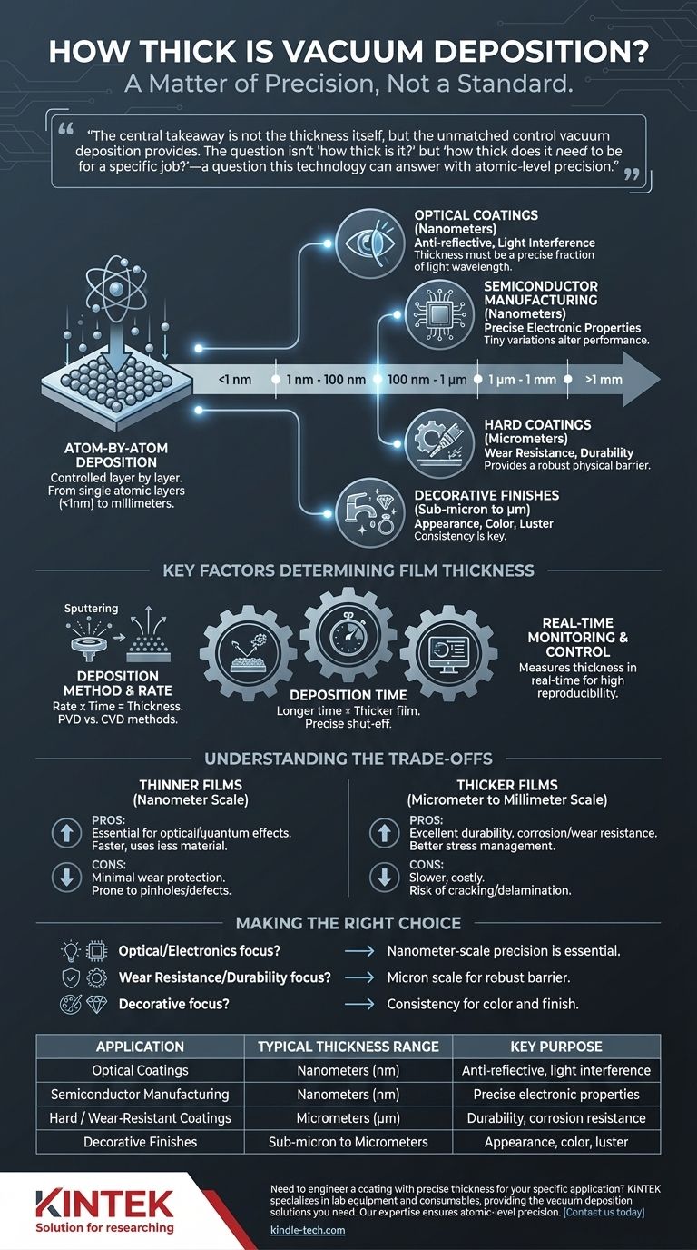
At its most fundamental, the thickness of a vacuum-deposited layer is not a single value but a precisely controlled parameter that can range from a single layer of atoms—less than a nanometer—to several millimeters. The specific thickness is entirely dependent on the intended function of the coating, whether it's for an optical lens, a durable tool, or a semiconductor chip. This process is defined by its precision, not by a standard thickness.
The central takeaway is not the thickness itself, but the unmatched control vacuum deposition provides. The question isn't "how thick is it?" but "how thick does it need to be for a specific job?"—a question this technology can answer with atomic-level precision.
Why Thickness is a Range, Not a Single Number
Vacuum deposition processes are fundamentally about building a material layer by layer. This bottom-up approach is what gives the technology its incredible versatility and precision.
The Principle of Atom-by-Atom Deposition
As the name implies, vacuum deposition works by depositing material atom-by-atom or molecule-by-molecule onto a surface. This happens in a high-vacuum chamber, which removes air and other particles that could interfere with the process.
Because you are controlling the flow of individual atoms, you can stop the process after any amount of time. This allows for the creation of films with thicknesses controlled down to the angstrom (one-tenth of a nanometer) or single atomic layer.
The Role of the Application
The final thickness is dictated entirely by the coating's purpose. There is no "one-size-fits-all" answer, as different functions require vastly different material thicknesses.
- Optical Coatings: For anti-reflective coatings on eyeglasses or camera lenses, thicknesses are incredibly precise, often in the nanometer range. The thickness must be a specific fraction of the wavelength of light to create the desired interference effect.
- Semiconductor Manufacturing: In fabricating microchips, layers of conductive or insulating materials are deposited with extreme precision. These films are also in the nanometer range, where even a tiny variation can alter the device's electronic properties.
- Hard Coatings: For adding wear resistance to cutting tools or engine parts, thicker coatings are needed. These films, often applied via Physical Vapor Deposition (PVD), are typically measured in micrometers (microns) to provide a durable barrier.
- Decorative Finishes: Coatings on faucets or jewelry are designed for appearance and some durability. Thickness here is less critical than for optical uses but is still controlled to achieve the right color and luster, often in the sub-micron range.
Key Factors That Determine Film Thickness
The final thickness of a vacuum-deposited film is a direct result of several controlled process variables. Engineers use these levers to achieve the exact specification required.
Deposition Method and Rate
The two main families of vacuum deposition are Physical Vapor Deposition (PVD) and Chemical Vapor Deposition (CVD). Different techniques within these families (like sputtering or evaporation) have characteristic deposition rates.
This rate—how much material lands on the surface over time—is a critical variable. For a stable process, the final thickness is simply a function of the deposition rate multiplied by the deposition time.
Deposition Time
This is the most straightforward control parameter. For a known, stable deposition rate, running the process for a longer time results in a thicker film. Automated systems can shut off the process with sub-second accuracy.
Real-Time Monitoring and Control
Modern deposition systems do not run blind. They include sophisticated instruments, such as deposition rate monitors, that measure the film's thickness in real time.
This feedback loop allows the system to adjust parameters on the fly or stop the process precisely when the target thickness is reached, ensuring high reproducibility and accuracy.
Understanding the Trade-offs
Choosing a film thickness involves balancing competing requirements. What makes a film good for one application can make it unsuitable for another.
Thinner Films (Nanometer Scale)
- Pros: Essential for optical and electronic properties where wave interference or quantum effects are critical. They are also faster and use less material to produce.
- Cons: Offer minimal protection against mechanical wear and abrasion. Extremely thin films can also suffer from defects like pinholes or a lack of continuous coverage.
Thicker Films (Micrometer to Millimeter Scale)
- Pros: Provide excellent durability, corrosion resistance, and wear protection. Internal stresses can sometimes be managed better over thicker films.
- Cons: Can be slow and costly to produce. The inherent stress in a thick film can build up and cause it to crack or delaminate. They are unsuitable for most optical or high-frequency electronic applications.
Making the Right Choice for Your Goal
The optimal thickness is the one that achieves your primary performance goal without adding unnecessary cost or negative side effects.
- If your primary focus is optical performance or electronics: You require nanometer-scale precision to control light or electricity, making thin-film control essential.
- If your primary focus is wear resistance and durability: You are operating in the micron scale, where a robust physical barrier is more important than atomic precision.
- If your primary focus is decorative appeal: You need consistency for color and finish, but the exact thickness is less critical than for technical applications.
Ultimately, vacuum deposition empowers you to engineer a surface for a specific function with unparalleled control.
Summary Table:
| Application | Typical Thickness Range | Key Purpose |
|---|---|---|
| Optical Coatings | Nanometers (nm) | Anti-reflective, light interference |
| Semiconductor Manufacturing | Nanometers (nm) | Precise electronic properties |
| Hard / Wear-Resistant Coatings | Micrometers (µm) | Durability, corrosion resistance |
| Decorative Finishes | Sub-micron to Micrometers | Appearance, color, luster |
Need to engineer a coating with precise thickness for your specific application? KINTEK specializes in lab equipment and consumables, providing the vacuum deposition solutions you need for optical, semiconductor, or durable tool coatings. Our expertise ensures you achieve atomic-level precision for superior performance. Contact us today to discuss your project requirements!
Visual Guide
Related Products
- Chemical Vapor Deposition CVD Equipment System Chamber Slide PECVD Tube Furnace with Liquid Gasifier PECVD Machine
- Molybdenum Tungsten Tantalum Evaporation Boat for High Temperature Applications
- Inclined Rotary Plasma Enhanced Chemical Vapor Deposition PECVD Equipment Tube Furnace Machine
- Inclined Rotary Plasma Enhanced Chemical Vapor Deposition PECVD Equipment Tube Furnace Machine
- HFCVD Machine System Equipment for Drawing Die Nano-Diamond Coating
People Also Ask
- How are carbon nanotubes grown? Master Scalable Production with Chemical Vapor Deposition
- What happens during deposition chemistry? Building Thin Films from Gaseous Precursors
- What types of substrates are used in CVD to facilitate graphene films? Optimize Graphene Growth with the Right Catalyst
- What are the advantages of chemical vapor deposition? Achieve Superior Thin Films for Your Lab
- What are the core advantages of PE-CVD in OLED encapsulation? Protect Sensitive Layers with Low-Temp Film Deposition