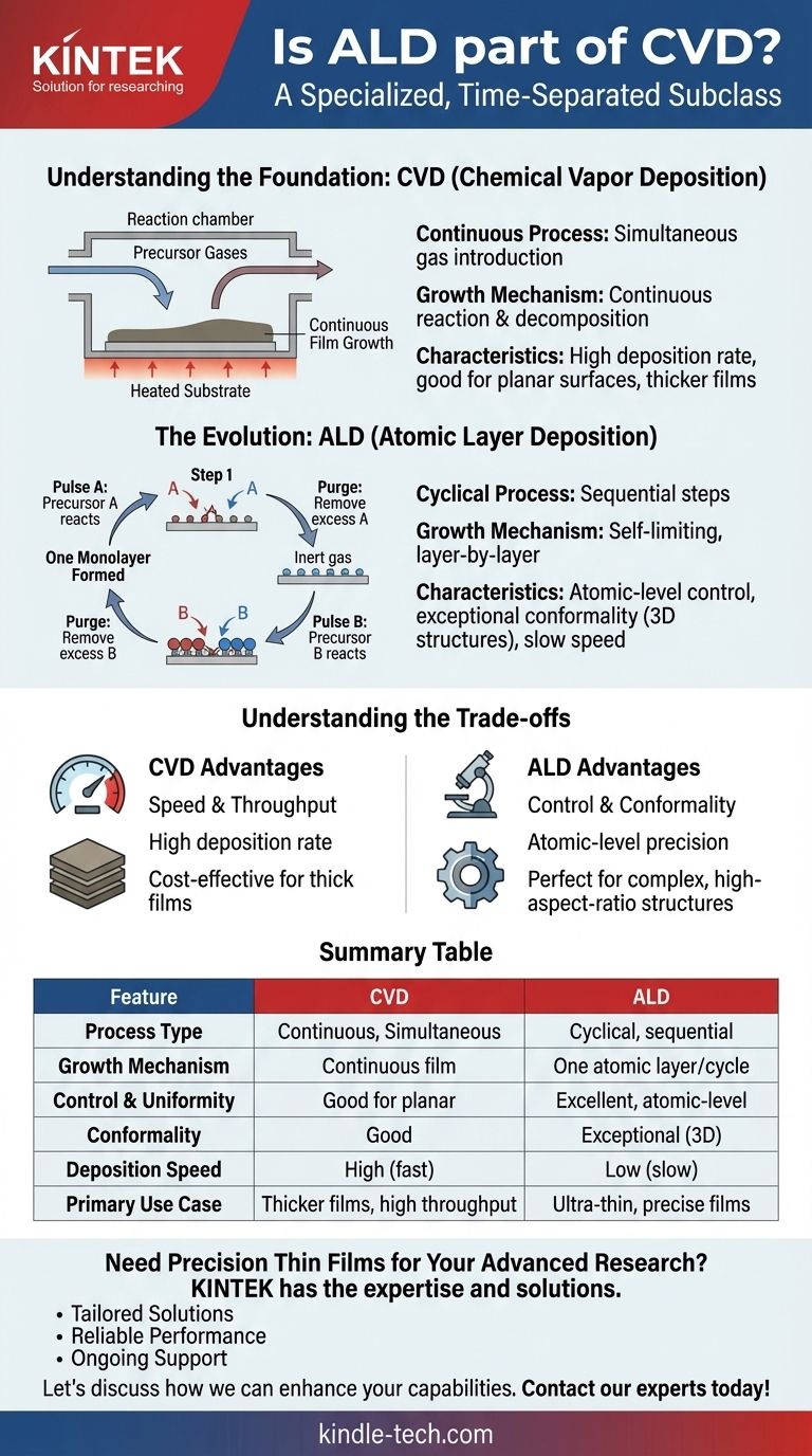
Technically speaking, Atomic Layer Deposition (ALD) is a specialized, time-separated subclass of Chemical Vapor Deposition (CVD). While it evolved from CVD principles and uses the same fundamental concept of precursor gases reacting to form a solid film, its unique, self-limiting cyclical process makes it distinct enough to be considered its own deposition category in practice.
The critical distinction is not in the chemistry but in the methodology. CVD is a continuous, simultaneous process, whereas ALD is a sequential, cyclical process that deposits material exactly one atomic layer at a time, offering unparalleled control.
Understanding the Foundation: Chemical Vapor Deposition (CVD)
The Continuous Process
In a traditional CVD process, one or more reactive precursor gases are introduced into a chamber simultaneously.
These gases flow continuously over a heated substrate.
How Growth Occurs
The heat energizes the gases, causing them to react and decompose on and near the substrate surface. This chemical reaction results in the deposition of a solid thin film.
Because the precursors are always present, the film grows continuously as long as the gas flow is maintained. This makes the process relatively fast.
The Evolution: Atomic Layer Deposition (ALD)
A Cyclical, Not Continuous, Approach
ALD breaks the continuous CVD reaction down into a series of discrete, sequential steps within a cycle.
A typical ALD cycle involves introducing the first precursor gas (Pulse A), which reacts with the substrate surface.
The Purge Step
Crucially, any excess, unreacted precursor from Pulse A is then completely removed from the chamber by an inert purge gas.
The Second Reaction
Next, a second precursor gas (Pulse B) is introduced. It reacts only with the layer of precursor A that is already bound to the surface.
This is followed by another purge step to remove excess precursor B, completing one full cycle and depositing a single, uniform monolayer of material.
The Self-Limiting Reaction
The power of ALD comes from its self-limiting nature. During each pulse, the precursor gas will only react with the available active sites on the surface.
Once all sites are occupied, the reaction naturally stops. This is why each cycle deposits exactly one atomic layer, regardless of minor variations in exposure time or precursor concentration.
Understanding the Trade-offs
Control and Conformality: ALD's Advantage
The self-limiting, layer-by-layer nature of ALD provides atomic-level control over film thickness and composition.
This process also yields exceptional conformality, meaning it can perfectly coat highly complex, 3D structures with deep trenches or pores (high-aspect-ratio structures) with a uniform film.
Speed and Throughput: CVD's Strength
The primary drawback of ALD is its speed. Building a film one atomic layer at a time is inherently slow.
CVD, being a continuous process, has a much higher deposition rate. This makes it far more practical and cost-effective for applications requiring thicker films where atomic-level precision is not the primary concern.
ALD vs. CVD: Choosing the Right Tool for the Job
Your choice between these related techniques depends entirely on the specific requirements of your application.
- If your primary focus is unparalleled precision and perfect uniformity, especially on complex 3D nanostructures, then ALD is the only viable choice.
- If your primary focus is high-speed deposition and creating thicker films where atomic-level precision is not the top priority, then CVD is the more efficient and economical method.
Understanding their fundamental relationship—one of specialization, not opposition—allows you to select the precise deposition method your application demands.
Summary Table:
| Feature | CVD (Chemical Vapor Deposition) | ALD (Atomic Layer Deposition) |
|---|---|---|
| Process Type | Continuous, simultaneous reaction | Cyclical, sequential pulses |
| Growth Mechanism | Continuous film growth | One atomic layer per cycle |
| Control & Uniformity | Good for planar surfaces | Excellent, atomic-level control |
| Conformality | Good | Exceptional (ideal for 3D structures) |
| Deposition Speed | High (fast) | Low (slow) |
| Primary Use Case | Thicker films, high throughput | Ultra-thin, precise films on complex shapes |
Need Precision Thin Films for Your Advanced Research?
Choosing the right deposition technique is critical for your project's success. Whether you require the high throughput of CVD systems or the atomic-level precision of ALD equipment, KINTEK has the expertise and solutions to meet your laboratory's unique needs.
We provide:
- Tailored Solutions: Expert guidance to select the perfect deposition system for your application.
- Reliable Performance: High-quality, durable lab equipment built for precision and repeatability.
- Ongoing Support: Comprehensive service and consumables to keep your research on track.
Let's discuss how we can enhance your capabilities. Contact our experts today to find the ideal thin-film deposition solution for your laboratory!
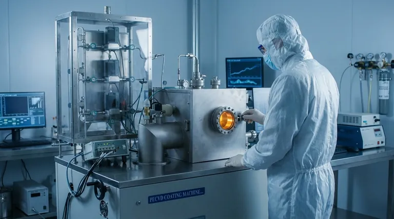
Visual Guide
Related Products
- Lab Electrochemical Workstation Potentiostat for Laboratory Use
- Thin-Layer Spectral Electrolysis Electrochemical Cell
People Also Ask
- How does an electrochemical testing system evaluate mesoporous oxide electrodes? Precision Analysis for Battery Research
- What are the primary functions of an electrochemical workstation (Potentiostat)? Expert Titanium Alloy Corrosion Analysis
- What role does a high-precision electrochemical workstation play in the leaching process of Sm2(Co,Fe,Cu,Zr)17 magnets?
- What is the significance of EIS testing for composite catalysts? Optimize Charge Transfer with Precision Workstations
- What role do electrochemical workstations play in researching the corrosion resistance of carbon coatings? Expert Guide