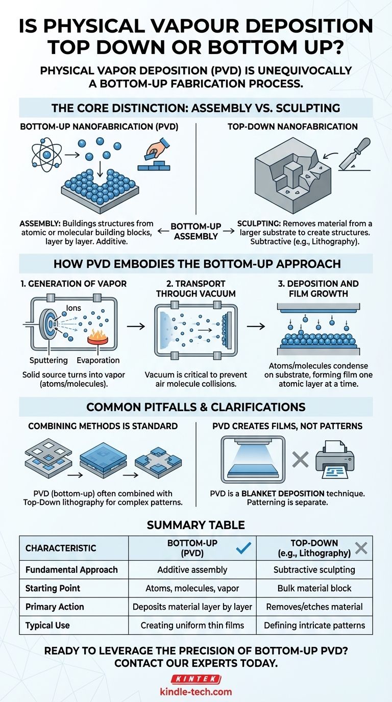
To be clear: Physical Vapor Deposition (PVD) is unequivocally a bottom-up fabrication process. This classification comes from its fundamental mechanism, which involves building a material layer by layer from its most basic constituents—atoms or molecules—rather than carving a structure out of a larger block.
The core distinction is one of strategy: bottom-up techniques like PVD assemble structures from atomic or molecular building blocks, while top-down techniques sculpt structures by removing material from a larger substrate.
The Core Principle: Assembly vs. Sculpting
To understand why PVD fits where it does, it's crucial to grasp the two fundamental approaches to nanofabrication.
Defining "Bottom-Up" Nanofabrication
Bottom-up fabrication starts with the smallest possible units—atoms, molecules, or clusters—and systematically assembles them into a larger, more complex structure.
Think of it as building a wall with individual bricks. Each brick (an atom) is placed precisely to create the final, desired form (the thin film). This method is additive by nature.
Defining "Top-Down" Nanofabrication
Top-down fabrication takes the opposite approach. It begins with a large piece of bulk material and uses subtractive processes, like carving or etching, to remove material until only the desired structure remains.
This is analogous to a sculptor starting with a block of marble and chipping away everything that isn't the final statue. Photolithography, the cornerstone of the semiconductor industry, is the classic example.
How PVD Embodies the Bottom-Up Approach
The PVD process is a perfect illustration of the bottom-up, or additive, manufacturing principle. It generally consists of three key stages.
1. Generation of Vapor
A solid source material, known as the "target," is converted into a vapor of individual atoms or molecules. This is typically achieved through sputtering (bombarding the target with energetic ions) or thermal evaporation (heating the material until it vaporizes).
2. Transport Through Vacuum
These vaporized particles travel through a low-pressure vacuum chamber from the source to the target object, known as the "substrate." The vacuum is critical to prevent these particles from colliding with air molecules.
3. Deposition and Film Growth
The atoms or molecules land on the substrate's surface and condense, forming a thin, solid film. The film grows in thickness one atomic layer at a time as more particles arrive, perfectly embodying the "building with bricks" analogy.
Common Pitfalls and Clarifications
Understanding the distinction is key, but it's also important to recognize how these methods are used in practice.
Combining Methods is Standard Practice
In real-world applications, especially semiconductor manufacturing, bottom-up and top-down techniques are almost always used together. PVD is not used in isolation to create complex patterns.
For example, to create metal wiring on a chip, a top-down lithography step first creates a patterned mask. Then, a bottom-up PVD step deposits a layer of metal over the entire surface. Finally, another process (like "lift-off" or etching) removes the unwanted metal, leaving behind the desired circuit pattern.
PVD Creates Films, Not Patterns
A common point of confusion is thinking PVD "prints" patterns. It does not. PVD is a blanket deposition technique that coats everything in its line of sight. The patterning and intricate shaping are handled by the top-down lithography and etching steps that precede or follow it.
Applying This to Your Goal
Your understanding of this concept directly impacts how you would approach a fabrication challenge.
-
If your primary focus is creating a uniform, high-purity thin film: You are using a pure bottom-up method. PVD is the ideal tool for depositing materials with precise, atomic-level control over thickness and composition.
-
If your primary focus is fabricating a complex micro-scale device (like a transistor): You will use a combination of approaches. You'll rely on top-down photolithography to define the pattern and bottom-up PVD to deposit the functional material layers within that pattern.
-
If your primary focus is controlling material properties at the nanoscale: The bottom-up nature of PVD is your advantage. By controlling deposition parameters, you directly influence the film's crystal structure, density, and stress at the atomic level.
Understanding the distinction between bottom-up assembly and top-down sculpting is fundamental to mastering modern fabrication.
Summary Table:
| Characteristic | Bottom-Up (PVD) | Top-Down (e.g., Lithography) |
|---|---|---|
| Fundamental Approach | Additive assembly | Subtractive sculpting |
| Starting Point | Atoms, molecules, vapor | Bulk material block |
| Primary Action | Deposits material layer by layer | Removes/etches material |
| Typical Use | Creating uniform thin films | Defining intricate patterns |
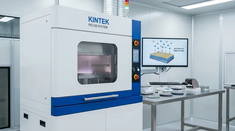
Ready to leverage the precision of bottom-up PVD in your lab? KINTEK specializes in high-performance lab equipment and consumables for all your deposition needs. Whether you're depositing uniform thin films or integrating PVD into a larger fabrication process, our expertise ensures you achieve superior material control and consistent results. Contact our experts today to discuss how our solutions can enhance your laboratory's capabilities!
Visual Guide
Related Products
- Chemical Vapor Deposition CVD Equipment System Chamber Slide PECVD Tube Furnace with Liquid Gasifier PECVD Machine
- RF PECVD System Radio Frequency Plasma-Enhanced Chemical Vapor Deposition RF PECVD
- Customer Made Versatile CVD Tube Furnace Chemical Vapor Deposition Chamber System Equipment
- Microwave Plasma Chemical Vapor Deposition MPCVD Machine System Reactor for Lab and Diamond Growth
- Custom CVD Diamond Coating for Lab Applications
People Also Ask
- What is plasma enhanced chemical vapor deposition PECVD equipment? A Guide to Low-Temperature Thin Film Deposition
- What happens during deposition chemistry? Building Thin Films from Gaseous Precursors
- What are the core advantages of PE-CVD in OLED encapsulation? Protect Sensitive Layers with Low-Temp Film Deposition
- What is the chemical vapor deposition growth process? Build Superior Thin Films from the Atom Up
- Why is Chemical Vapor Deposition (CVD) equipment uniquely suited for constructing hierarchical superhydrophobic structures?


