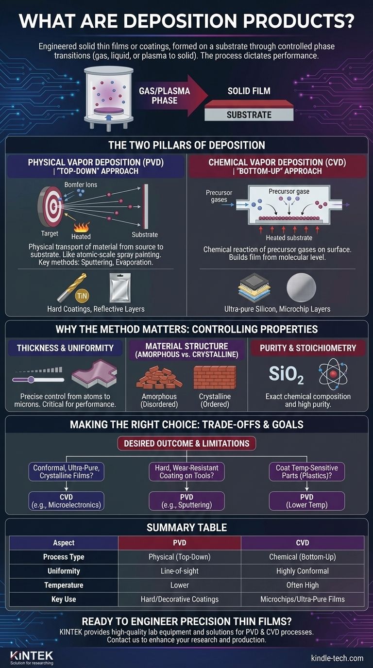
In materials science and engineering, a deposition product is the solid material, typically a thin film or coating, that is intentionally formed on a surface (known as a substrate). This is achieved through a controlled process where a material is transitioned from a gas, liquid, or plasma phase into a solid layer. The "product" is this newly formed layer, whose properties are precisely engineered for a specific function.
The term "deposition product" refers less to a specific substance and more to the result of a highly controlled engineering process. The value and function of the product are defined not just by what material it is, but by how it was deposited, which dictates its atomic structure, purity, and performance.
The Two Pillars of Deposition: PVD and CVD
Nearly all advanced deposition products are created using one of two core methodologies: Physical Vapor Deposition (PVD) or Chemical Vapor Deposition (CVD). Understanding the difference is critical to understanding the product itself.
Physical Vapor Deposition (PVD): The "Top-Down" Approach
PVD works by physically moving material from a source (a "target") to the substrate. Imagine it as a form of atomic-scale spray painting.
The two main PVD methods are sputtering and evaporation. In sputtering, high-energy ions bombard the target, knocking atoms loose, which then travel and coat the substrate. In evaporation, the source material is heated in a vacuum until it vaporizes, and this vapor condenses on the cooler substrate.
Common PVD products include the hard, gold-colored titanium nitride (TiN) coatings on drill bits or the thin metal layers that give potato chip bags their reflective interior.
Chemical Vapor Deposition (CVD): The "Bottom-Up" Approach
CVD is a chemical process. It builds the film atom-by-atom from reactive gases known as "precursors."
These precursor gases are introduced into a reaction chamber where they decompose and react on the heated substrate's surface, leaving behind the desired solid material. Think of it like frost forming on a cold window, where water vapor (the precursor) turns directly into a solid crystal layer (the ice).
CVD is essential for creating the ultra-pure silicon and silicon dioxide layers that form the basis of all modern microchips.
Why the Deposition Method Matters
The choice between PVD, CVD, or their many variants is a deliberate engineering decision. The method directly controls the final properties of the deposition product.
Controlling Thickness and Uniformity
Deposition processes allow for incredible precision. By controlling parameters like time, temperature, and gas pressure, engineers can create films of a specific thickness, from a few atoms to many microns, with remarkable uniformity across the substrate's surface.
This control is non-negotiable for products like optical filters or semiconductor wafers, where even tiny variations in thickness can lead to complete device failure.
Defining Material Structure (Amorphous vs. Crystalline)
The deposition conditions, especially temperature, determine how the atoms arrange themselves.
A crystalline structure is highly ordered, like a perfectly stacked wall of bricks. This often leads to specific electronic or optical properties. In contrast, an amorphous structure is disordered, like a pile of bricks, which can be desirable for creating smooth, uniform surfaces.
Ensuring Purity and Stoichiometry
The final product must have the correct chemical composition, or stoichiometry. For example, a silicon dioxide (SiO₂) film must have exactly two oxygen atoms for every one silicon atom.
CVD excels at producing high-purity, stoichiometric films because it builds them from precise chemical reactions. However, both PVD and CVD are performed in vacuum chambers to minimize contamination from unwanted atmospheric gases, which would otherwise be incorporated as impurities.
Understanding the Trade-offs
Neither method is universally superior; each comes with fundamental trade-offs that make them suitable for different applications.
PVD: Line-of-Sight and Lower Temperatures
PVD is fundamentally a line-of-sight process. The sputtered or evaporated atoms travel in straight lines, making it difficult to evenly coat complex, three-dimensional shapes with hidden surfaces.
However, many PVD processes can run at lower temperatures than CVD. This makes PVD ideal for coating heat-sensitive materials, such as plastics or previously fabricated electronic components.
CVD: Conformality vs. High Heat and Hazards
CVD is not limited by line-of-sight and can produce highly conformal coatings that uniformly cover even the most complex 3D structures. This is a major advantage in microfabrication.
The primary drawback is heat. Many CVD processes require very high temperatures that the substrate may not be able to withstand. Furthermore, the precursor gases used are often highly toxic, flammable, or corrosive, requiring extensive and costly safety infrastructure.
Making the Right Choice for Your Goal
The ideal deposition method is determined entirely by the desired properties of your final product and the physical and chemical limitations of your substrate.
- If your primary focus is creating ultra-pure, conformal crystalline films for electronics: CVD is often the superior choice due to its precise control over chemical reactions at the atomic level.
- If your primary focus is applying a hard, wear-resistant coating onto metal tools or parts: PVD processes like sputtering are more practical, often lower temperature, and highly effective.
- If your primary focus is metallizing a temperature-sensitive plastic part for decorative or shielding purposes: PVD is the clear choice because its lower processing temperatures will not melt or damage the substrate.
Ultimately, understanding deposition is about mastering the process to engineer the exact material properties you need.
Summary Table:
| Aspect | PVD (Physical Vapor Deposition) | CVD (Chemical Vapor Deposition) |
|---|---|---|
| Process Type | Physical (e.g., sputtering, evaporation) | Chemical (gas-phase reactions) |
| Coating Uniformity | Line-of-sight; less conformal | Highly conformal; covers complex 3D shapes |
| Temperature Requirements | Lower temperatures; suitable for heat-sensitive substrates | Often high temperatures; may damage sensitive materials |
| Common Applications | Hard coatings (e.g., TiN on tools), decorative metallization | Microchips, ultra-pure silicon layers, optical films |
| Key Advantages | Lower heat, simpler for flat surfaces | High purity, precise stoichiometry, excellent conformality |
Ready to engineer precision thin films for your lab?
At KINTEK, we specialize in providing high-quality lab equipment and consumables for deposition processes, including PVD and CVD systems. Whether you're developing microelectronics, advanced optics, or durable coatings, our solutions ensure precise control over thickness, purity, and material structure.
Contact us today to discuss how our expertise can enhance your research and production outcomes!
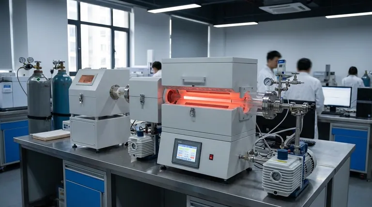
Visual Guide
Related Products
- RF PECVD System Radio Frequency Plasma-Enhanced Chemical Vapor Deposition RF PECVD
- Evaporation Boat for Organic Matter
- Laboratory CVD Boron Doped Diamond Materials
People Also Ask
- What is plasma chemical vapor deposition? A Low-Temperature Thin Film Coating Solution
- How does Radio Frequency Enhanced Plasma Chemical Vapour Deposition (RF-PECVD) work? Learn the Core Principles
- What is plasma enhanced chemical vapour deposition PECVD used for? Enable Low-Temp Thin Films for Electronics & Solar
- What is plasma enhanced chemical Vapour deposition process used for fabrication of? A Guide to Low-Temperature Thin Films
- What is plasma CVD? Unlock Low-Temperature Thin Film Deposition for Sensitive Materials


