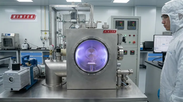
At their core, sputtering tools are highly controlled systems for depositing ultra-thin films of material onto a surface. These tools use a physical vapor deposition (PVD) process where a high-energy plasma bombards a source material, called a target, knocking individual atoms loose. These ejected atoms then travel through a vacuum and coat a designated substrate, creating a film with exceptional purity, uniformity, and adhesion.
Sputtering is not a single process but a family of sophisticated vacuum-based techniques. Its primary value lies in its ability to produce highly uniform, dense, and strongly adhered thin films, making it a cornerstone technology for manufacturing advanced products like semiconductors, optical lenses, and hard coatings.
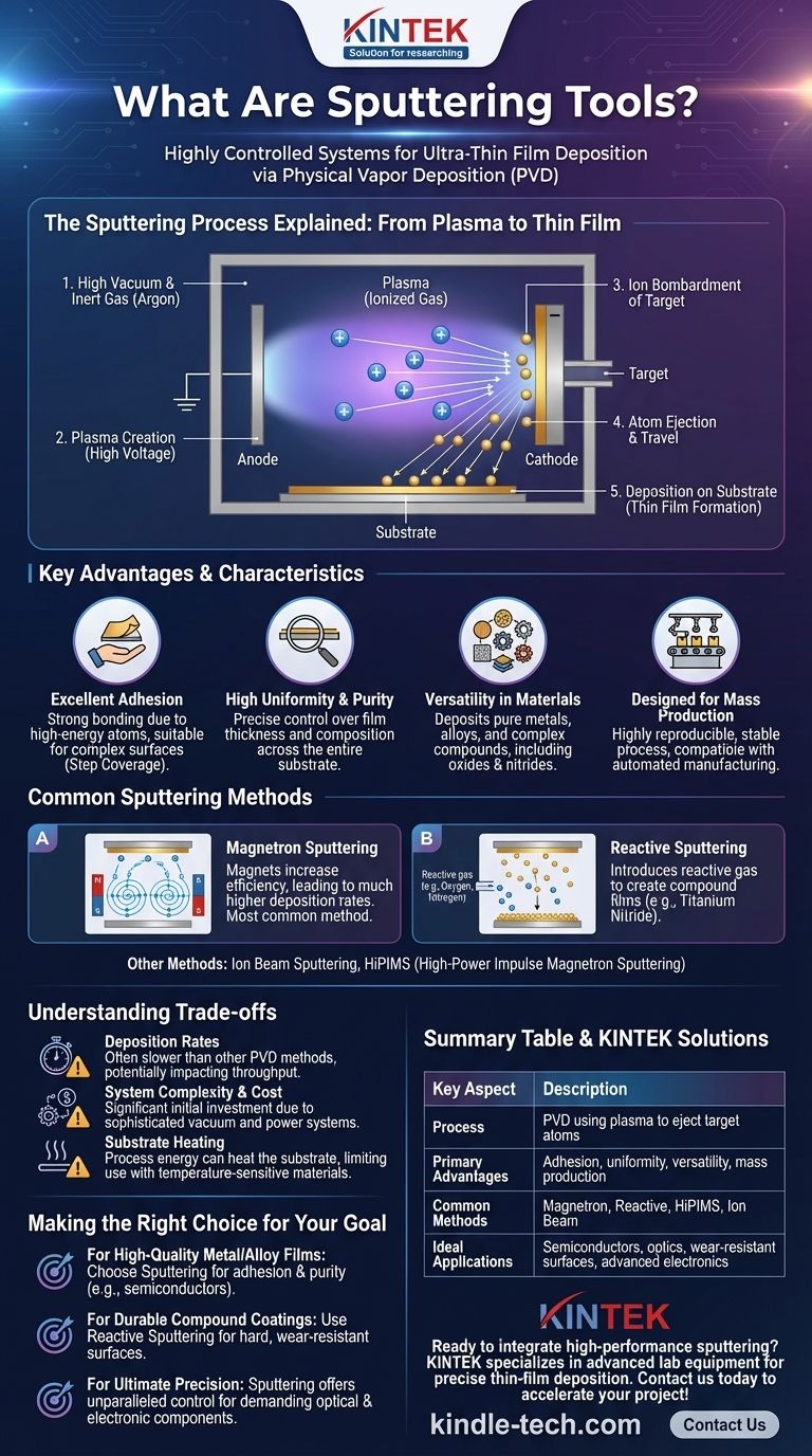
How Sputtering Fundamentally Works
Sputtering operates on the principle of momentum transfer. The process takes place inside a sealed vacuum chamber to ensure the purity of the deposited film.
The Core Mechanism: Plasma and Ion Bombardment
First, the chamber is pumped down to a high vacuum and then backfilled with a small amount of an inert process gas, typically Argon. A high voltage is applied, which ignites the gas and creates a glowing, ionized state of matter known as plasma.
The positively charged Argon ions in the plasma are accelerated by an electric field, causing them to collide with the negatively charged target (the source material). This bombardment has enough energy to physically knock out, or "sputter," atoms from the target's surface.
Deposition Onto the Substrate
These sputtered atoms travel in a straight line through the vacuum until they land on the substrate (the item being coated). Upon arrival, they condense and build up, layer by layer, to form a thin, solid film.
Key Characteristics and Advantages
The nature of the sputtering process provides several distinct advantages that make it suitable for high-performance applications.
Excellent Adhesion and Step Coverage
Sputtered atoms arrive at the substrate with significant kinetic energy. This energy promotes strong bonding to the surface, resulting in excellent film adhesion. It also allows the atoms to coat complex, non-flat surfaces uniformly, a property known as step coverage.
High Uniformity and Purity
The process allows for precise control over the deposition rate and film thickness. This results in excellent film uniformity across the entire substrate, which is critical for applications in optics and electronics.
Versatility in Materials
Sputtering can be used to deposit a vast range of materials, including pure metals, alloys, and compounds. By using multiple targets or a single alloy target, complex alloy films can be created with precise compositions.
Designed for Mass Production
The process is highly reproducible and stable, with time and power being easily controlled. Combined with the infrequent need for target replacement, these factors make sputtering technology highly compatible with automated, high-volume manufacturing.
Common Sputtering Methods and Variations
Different sputtering techniques have been developed to optimize the process for specific materials and applications.
Magnetron Sputtering
This is the most common method. Magnets are placed behind the target to create a magnetic field that traps electrons near the target surface. This dramatically increases the ion bombardment efficiency, leading to much higher deposition rates compared to simple diode sputtering.
Reactive Sputtering
This technique is used to create compound films. It involves sputtering a metal target in the presence of a reactive gas like oxygen or nitrogen. For example, sputtering a titanium target in a nitrogen environment will deposit a hard, wear-resistant titanium nitride (TiN) film on the substrate.
Other Key Methods
Other specialized techniques exist, such as ion beam sputtering for ultimate film purity and density, and High-Power Impulse Magnetron Sputtering (HiPIMS) for creating exceptionally dense films with superior adhesion.
Understanding the Trade-offs
While powerful, sputtering is not the ideal solution for every thin-film application. Understanding its limitations is key to making an informed decision.
Deposition Rates
Even with magnetron enhancement, sputtering can be a relatively slow process compared to other PVD methods like thermal evaporation, especially for certain materials. This can impact throughput in some production environments.
System Complexity and Cost
Sputtering systems are sophisticated pieces of equipment. They require high-vacuum chambers, high-voltage power supplies, cooling systems, and precise gas flow control, making the initial capital investment significant.
Substrate Heating
The energy imparted by the condensing atoms and plasma can cause the substrate to heat up during deposition. This can be a limiting factor when coating temperature-sensitive materials like plastics or certain biological samples.
Making the Right Choice for Your Goal
Selecting the right deposition method depends entirely on the required film properties and production constraints.
- If your primary focus is high-quality metal or alloy films: Sputtering is an exceptional choice for applications demanding strong adhesion and high purity, such as in semiconductor manufacturing or for creating reflective coatings.
- If your primary focus is durable compound coatings: Reactive sputtering is the go-to method for efficiently depositing hard or dielectric films like oxides and nitrides for wear resistance or optical filters.
- If your primary focus is ultimate precision over speed: Sputtering offers unparalleled control over film thickness, uniformity, and density, making it ideal for the most demanding optical and electronic components where performance cannot be compromised.
Ultimately, sputtering is a foundational technology that enables the engineering of materials at the atomic scale, making it indispensable for modern technological advancement.
Summary Table:
| Key Aspect | Description |
|---|---|
| Process | Physical Vapor Deposition (PVD) using plasma to eject target atoms onto a substrate. |
| Primary Advantages | Excellent film adhesion, high uniformity, material versatility, and mass production capability. |
| Common Methods | Magnetron Sputtering, Reactive Sputtering, HiPIMS, Ion Beam Sputtering. |
| Ideal Applications | Semiconductors, optical coatings, wear-resistant surfaces, and advanced electronics. |
Ready to integrate high-performance sputtering into your lab? KINTEK specializes in advanced lab equipment and consumables for precise thin-film deposition. Whether you're developing semiconductors, optical components, or specialized coatings, our sputtering solutions deliver the purity, uniformity, and adhesion your research demands. Contact us today to discuss how our expertise can accelerate your project!
Visual Guide
Related Products
- Professional Cutting Tools for Carbon Paper Cloth Diaphragm Copper Aluminum Foil and More
- Three-dimensional electromagnetic sieving instrument
- Single Punch Manual Tablet Press Machine TDP Tablet Punching Machine
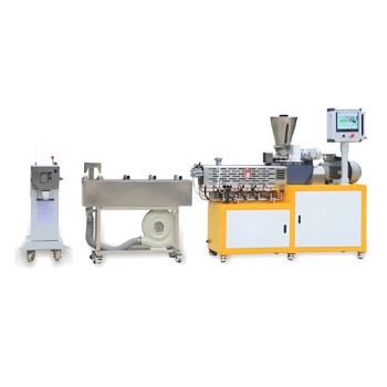
- Twin Screw Extruder Plastic Granulation Machine
- Multi-Punch Rotary Tablet Press Mold Ring for Rotating Oval and Square Molds
People Also Ask
- What are carbon cloths used for? Conquer Static Dust on Electronics & Screens
- How is carbon paper constructed? The Engineered Porous Scaffold for High-Performance Applications
- Why is carbon paper placed between the powder and the graphite mold? Protect Your LTPO Electrolytes & Tooling
- What are the typical uses for carbon paper? Powering Fuel Cells and Advanced Research
- How should carbon paper be handled during cutting? Prevent Fractures with a Delicate, Precise Approach