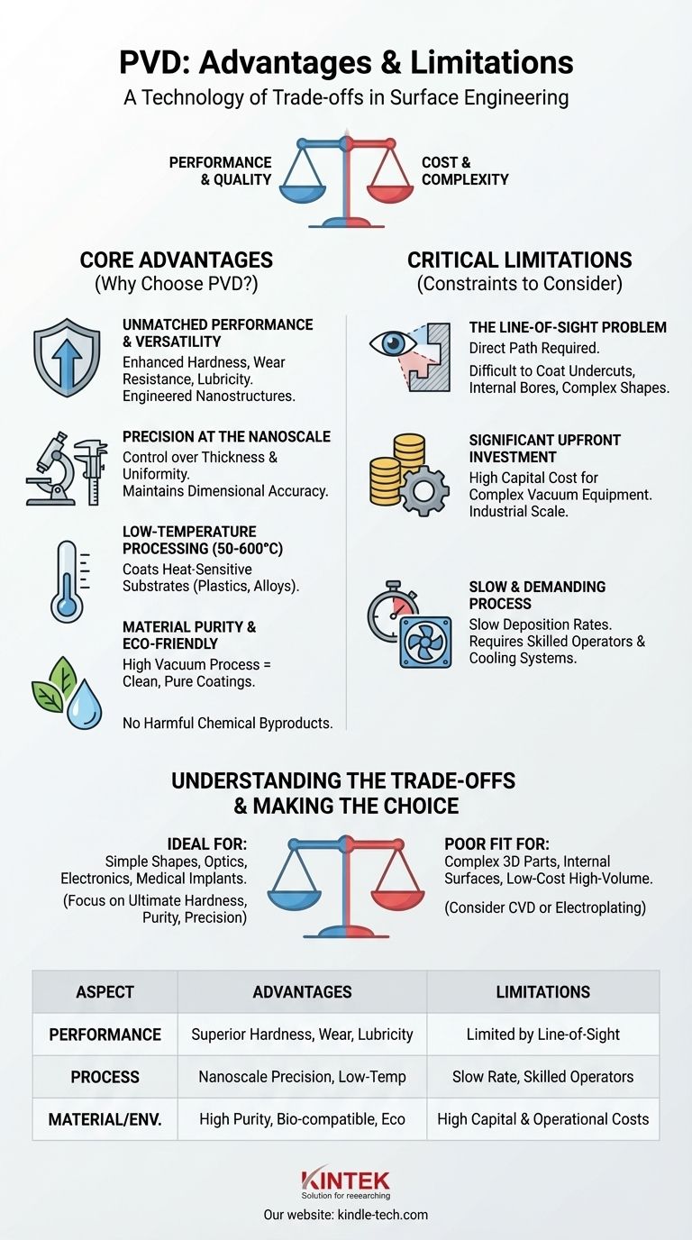
At its core, Physical Vapor Deposition (PVD) is a technology of trade-offs. It excels at creating exceptionally hard, thin, and pure coatings on a substrate, but these high-performance characteristics come with significant constraints related to process complexity, cost, and component geometry. This makes PVD a superior choice for specific applications while being unsuitable for others.
PVD is not a one-size-fits-all solution. It is a high-precision, high-investment surface engineering process best suited for applications where superior surface performance is critical and the component's geometry allows for direct line-of-sight coating.
The Core Advantages: Why Choose PVD?
The primary reason to select PVD is to dramatically enhance the surface properties of a material, granting it characteristics it does not naturally possess.
Unmatched Performance and Versatility
PVD coatings act as a formidable barrier against wear and friction. They can drastically increase the hardness and lubricity of a surface, which is why they are a mainstay for cutting tools and high-wear components.
This process allows for highly engineered layer structures, including monolayers, multilayers, and even complex nanostructures, enabling fine-tuned performance for specific needs.
Precision at the Nanoscale
PVD offers exceptional control over coating thickness and uniformity, making it possible to apply films in the nanometer range. This precision is critical for advanced applications.
The process maintains very good dimensional accuracy, meaning it doesn't significantly alter the part's size or shape. It also faithfully replicates the substrate's finish, whether it's a highly polished or a textured surface.
Low-Temperature Processing
Unlike some other coating methods, many PVD processes can be conducted at relatively low temperatures (50-600°C). This is a crucial advantage.
It allows for coating heat-sensitive substrates, such as plastics or certain metal alloys, that would be damaged or structurally altered by high-temperature treatments.
Material Purity and Environmental Friendliness
The PVD process occurs in a high vacuum, resulting in extremely pure and clean coatings with excellent adhesion. This makes it an ideal method for medical and surgical implants where biocompatibility is paramount.
It is also considered an environmentally friendly technology, as it does not produce the harmful chemical byproducts associated with traditional plating processes like electroplating.
The Limitations: Critical Constraints to Consider
While powerful, PVD is governed by strict physical and economic limitations that you must factor into your decision.
The Line-of-Sight Problem
The most significant operational constraint of PVD is that it is a line-of-sight technique. The coating material travels in a straight line from the source to the substrate.
This means it is very difficult to coat undercuts, internal bores, or complex three-dimensional shapes uniformly. Areas that are "in shadow" will receive little to no coating.
Significant Upfront Investment
PVD equipment is complex and expensive. The high vacuum chambers, power supplies, and control systems represent a high capital cost.
This generally positions PVD as a technology for industrial-scale production rather than small-scale or hobbyist applications.
Slow and Demanding Process
The rate of coating deposition is typically very slow, making it less suitable for applications requiring high-volume, rapid throughput.
Furthermore, the process requires a high vacuum and, in some cases, high temperatures, which necessitates skilled operators for proper execution and maintenance. The need for heat also often requires integrated cooling systems to protect the equipment and substrate.
Understanding the Trade-offs
Choosing PVD requires balancing its benefits against its inherent compromises.
Performance vs. Geometry
You gain exceptional hardness, wear resistance, and purity, but only on the surfaces that the vapor stream can physically reach. For simple geometries like drill bits or optical lenses, this is not an issue. For complex parts like an engine block, it is a non-starter.
Quality vs. Cost and Speed
The high-quality, pure, and precise coatings that PVD produces are a direct result of its controlled but slow and expensive process. If your primary driver is low cost or high speed, PVD is likely the wrong choice. If quality and performance are paramount, the cost may be justified.
Method-Specific Variations
"PVD" is a family of processes (e.g., sputtering, thermal evaporation). Each has its own trade-offs. For example, thermal evaporation can be faster and cheaper but is limited to materials with low melting points, while sputtering offers a wider range of materials at the cost of complexity.
Making the Right Choice for Your Application
Your final decision must be aligned with your project's primary goal.
- If your primary focus is ultimate surface hardness and wear resistance on simple shapes: PVD is a leading choice for applications like cutting tools, dies, and molds.
- If your primary focus is creating pure, precise thin films for optics or electronics: PVD is the industry standard for its unmatched control over thickness and material purity.
- If your primary focus is coating complex 3D parts with internal surfaces: The line-of-sight limitation makes PVD a poor fit; consider alternatives like Chemical Vapor Deposition (CVD) or electroplating.
- If your primary focus is low cost and high-speed production for non-critical surfaces: PVD's high capital investment and slow deposition rates make it economically unviable.
Ultimately, PVD is a specialized tool for achieving superior surface engineering, provided you can work within its significant operational constraints.
Summary Table:
| Aspect | Advantages | Limitations |
|---|---|---|
| Performance | Superior hardness, wear resistance, and lubricity | Limited by line-of-sight coating |
| Process Control | Nanoscale precision, low-temperature options | Slow deposition rate, requires skilled operators |
| Material & Environment | High purity, environmentally friendly, biocompatible | High capital investment and operational costs |
| Application Suitability | Ideal for optics, electronics, medical implants | Unsuitable for complex 3D shapes with undercuts |
Ready to enhance your lab's capabilities with precision coatings? KINTEK specializes in advanced lab equipment and consumables, including PVD solutions tailored for research and industrial applications. Whether you're working on cutting tools, medical devices, or electronic components, our expertise ensures you get the right equipment for superior surface performance. Contact us today to discuss how we can support your laboratory needs!
Visual Guide
Related Products
- RF PECVD System Radio Frequency Plasma-Enhanced Chemical Vapor Deposition RF PECVD
- Split Chamber CVD Tube Furnace with Vacuum Station Chemical Vapor Deposition System Equipment Machine
- Chemical Vapor Deposition CVD Equipment System Chamber Slide PECVD Tube Furnace with Liquid Gasifier PECVD Machine
- Molybdenum Tungsten Tantalum Special Shape Evaporation Boat
- VHP Sterilization Equipment Hydrogen Peroxide H2O2 Space Sterilizer
People Also Ask
- What are the advantages of PECVD? Enable Low-Temperature, High-Quality Thin-Film Deposition
- How does RF power create plasma? Achieve Stable, High-Density Plasma for Your Applications
- What are the benefits of PECVD? Achieve Superior Low-Temperature Thin Film Deposition
- What is an example of PECVD? RF-PECVD for High-Quality Thin Film Deposition
- What are the applications of PECVD? Essential for Semiconductors, MEMS, and Solar Cells