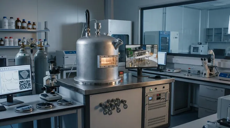
At its core, nanotechnology uses thin films to engineer materials with entirely new properties for applications ranging from advanced electronics to renewable energy. These ultra-thin layers, often just a few atoms thick, are fundamental building blocks in micro-electromechanical systems (MEMS), integrated circuit chips, photovoltaic solar cells, and high-efficiency batteries.
The crucial insight is that a material in the form of a thin film does not behave like its bulk counterpart. By reducing a material's structure to the nanoscale, its fundamental electrical, optical, and mechanical properties change, allowing us to build smaller, more efficient, and more powerful devices.
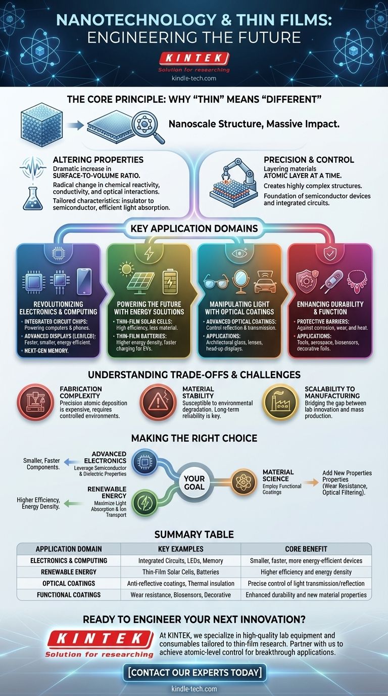
The Core Principle: Why "Thin" Means "Different"
The power of thin films in nanotechnology isn't just about making things smaller. It's about fundamentally changing how a material functions by controlling its structure at the atomic level.
Altering Properties at the Nanoscale
When a material is reduced to a thin film, its surface-to-volume ratio increases dramatically. This means a much larger proportion of its atoms are on the surface, which can radically alter its chemical reactivity, conductivity, and interaction with light.
This effect allows engineers to create materials with precisely tailored characteristics, such as turning an insulator into a semiconductor or making a material absorb light more efficiently.
Precision and Control
Thin film deposition techniques allow for the creation of highly complex structures by layering different materials one atomic layer at a time. This level of precision is the basis for modern semiconductor devices and integrated circuits.
By stacking various thin films, we can construct devices with specific functions, such as transistors, light-emitting diodes (LEDs), and computer memory cells.
Key Application Domains
The unique properties of thin films have made them indispensable across numerous high-technology sectors. They are not a niche material but a foundational platform for innovation.
Revolutionizing Electronics and Computing
Thin films are the bedrock of the entire digital world. They are used to create the microscopic transistors and pathways inside integrated circuit chips that power computers and mobile phones.
Their applications extend to LED and LCD displays, touch panels, and next-generation computer memory, enabling devices that are faster, smaller, and more energy-efficient.
Powering the Future with Energy Solutions
In the energy sector, thin-film photovoltaic cells are designed to capture sunlight with exceptional efficiency while using significantly less material than traditional solar panels.
Similarly, thin-film batteries offer the potential for higher energy density and faster charging, which is critical for electric vehicles and portable electronics.
Manipulating Light with Optical Coatings
Thin films are used to create advanced optical coatings that control the reflection and transmission of light. These are found on everything from anti-reflective coatings on eyeglasses to specialized mirrors and thermal insulation on architectural glass.
This technology is also essential for head-up displays in cars and high-performance optical lenses.
Enhancing Durability and Function
Beyond electronics, thin films serve as powerful functional coatings. They can create protective barriers against corrosion and wear on tools or act as thermal barriers in demanding aerospace applications.
These films are also used for decorative coatings on jewelry, freshness-preserving packaging foils, and even in advanced biosensors.
Understanding the Trade-offs and Challenges
While thin films offer remarkable advantages, their application is not without complexity. Understanding these challenges is key to successful implementation.
Fabrication Complexity
Depositing a perfectly uniform, defect-free film that is only a few atoms thick is a significant engineering challenge. The process requires highly controlled environments and sophisticated equipment, which can be expensive.
Material Stability
An extremely thin layer of material can be more susceptible to degradation from environmental factors like heat, moisture, and oxidation. Ensuring the long-term stability and reliability of these films is a primary concern in device engineering.
Scalability to Manufacturing
A technique that works perfectly in a research lab may be difficult or cost-prohibitive to scale up for mass production. Bridging the gap between nanoscale innovation and industrial-scale manufacturing remains a constant focus.
Making the Right Choice for Your Goal
The application of thin films is dictated by the specific material property you need to engineer for a given purpose.
- If your primary focus is advanced electronics: You will leverage thin films for their unique semiconductor and dielectric properties to build smaller, faster components.
- If your primary focus is renewable energy: You will use thin films to maximize light absorption in solar cells or improve ion transport in batteries.
- If your primary focus is material science: You will employ thin films as functional coatings to add new properties like wear resistance or optical filtering to existing materials.
Ultimately, thin films are the essential tool that allows us to build with atoms, turning the fundamental properties of matter into solutions for our most complex technological challenges.
Summary Table:
| Application Domain | Key Examples | Core Benefit |
|---|---|---|
| Electronics & Computing | Integrated Circuits, LEDs, Memory | Smaller, faster, more energy-efficient devices |
| Renewable Energy | Thin-Film Solar Cells, Batteries | Higher efficiency and energy density |
| Optical Coatings | Anti-reflective coatings, Thermal insulation | Precise control of light transmission/reflection |
| Functional Coatings | Wear resistance, Biosensors, Decorative | Enhanced durability and new material properties |
Ready to Engineer Your Next Innovation with Thin Films?
At KINTEK, we understand that the success of your nanotechnology project hinges on precision and reliability. Whether you are developing advanced semiconductors, next-generation solar cells, or durable protective coatings, the right lab equipment is crucial.
We specialize in providing high-quality lab equipment and consumables tailored to the demanding needs of thin-film research and development. By partnering with us, you gain access to the tools necessary to achieve the atomic-level control required for breakthrough applications in electronics, energy, and material science.
Let's build the future together. Contact our experts today to discuss how KINTEK can support your laboratory's specific thin-film application needs.
Visual Guide
Related Products
- Aluminum-Plastic Flexible Packaging Film for Lithium Battery Packaging
- Thin-Layer Spectral Electrolysis Electrochemical Cell
People Also Ask
- What are the three types of lamination? Choose the Perfect Finish for Your Print Project
- What is the thinnest coating? Unlocking Unique Properties at the Atomic Scale
- How to check if a lithium battery is good? Safely Test Voltage, Capacity & Internal Resistance
- Is there a way to test lithium batteries? Understand Voltage vs. True Health
- What are the properties of Aluminium (Al) relevant to its use in coatings? High Reflectivity & Conductivity Explored

