In essence, plasma deposition uses energized gas (plasma) to either physically knock atoms off a source target or to chemically assemble a film from gas molecules. The main types of plasma deposition fall into two primary families: Physical Vapor Deposition (PVD), most notably sputtering, and Plasma-Enhanced Chemical Vapor Deposition (PECVD).
The core distinction is simple: PVD methods like sputtering use plasma to physically transfer material from a solid target to your substrate. In contrast, PECVD uses plasma to drive chemical reactions from precursor gases, forming a new material directly on your substrate.
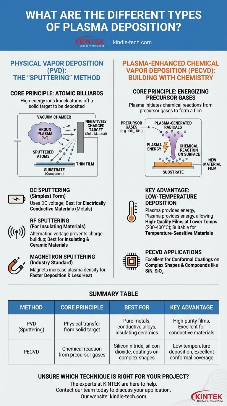
Physical Vapor Deposition (PVD): The "Sputtering" Method
The process described in your reference—using high-energy particles to liberate atoms from a target—is a perfect description of sputtering, a major category of PVD. Think of it as a game of atomic-scale billiards.
The Core Principle: Atomic Billiards
In sputtering, a high voltage is applied in a vacuum chamber, creating a plasma from an inert gas like Argon. These positively charged Argon ions are accelerated toward a negatively charged plate of the material you wish to deposit, called the target.
The ions strike the target with such force that they knock off, or "sputter," individual atoms. These neutral atoms travel through the chamber and deposit onto your component, known as the substrate, forming a thin, uniform film.
DC Sputtering: The Simplest Form
Direct Current (DC) sputtering is the most basic form. It uses a simple DC voltage to accelerate the ions.
This method works extremely well for depositing electrically conductive materials like pure metals (aluminum, titanium, tantalum) and some conductive compounds.
RF Sputtering: For Insulating Materials
If you try to use DC sputtering on an insulating (dielectric) material like titanium dioxide or silicon dioxide, positive charge builds up on the target's surface. This buildup eventually repels the incoming Argon ions, stopping the process.
Radio Frequency (RF) sputtering solves this by rapidly alternating the voltage. This alternating field prevents charge accumulation, allowing for the effective deposition of insulating and ceramic materials.
Magnetron Sputtering: The Industry Standard
Magnetron sputtering is an enhancement that can be applied to both DC and RF systems. It places powerful magnets behind the target.
These magnets trap electrons near the target's surface, creating a much denser, more intense plasma. This significantly increases the sputtering rate, leading to faster deposition and less heat damage to the substrate, making it the dominant method in modern industry.
Plasma-Enhanced Chemical Vapor Deposition (PECVD): Building with Chemistry
PECVD operates on a completely different principle. It does not use a solid target. Instead, it uses plasma to initiate a chemical reaction.
The Core Principle: Energizing Precursor Gases
In PECVD, volatile precursor gases are introduced into the vacuum chamber. For example, to deposit silicon nitride, you might use silane (SiH₄) and ammonia (NH₃) gases.
The plasma's energy breaks these gas molecules into highly reactive fragments called radicals. These radicals then react on the substrate surface, building the desired film atom by atom.
The Key Advantage: Low-Temperature Deposition
Traditional Chemical Vapor Deposition (CVD) requires very high temperatures (often >800°C) to drive the chemical reactions.
PECVD is revolutionary because the plasma provides the energy, not just heat. This allows for the deposition of high-quality films at much lower temperatures (typically 200-400°C), making it possible to coat temperature-sensitive materials like plastics or finished electronic devices.
Understanding the Trade-offs
Neither method is universally superior; the best choice depends entirely on your material and application requirements.
PVD (Sputtering): Purity vs. Complexity
Sputtering can produce very pure films, as you are physically transferring material from a high-purity target.
However, it is a "line-of-sight" process. It can be difficult to uniformly coat complex, three-dimensional shapes. Controlling the precise chemical ratio (stoichiometry) of complex compound films can also be challenging.
PECVD: Versatility vs. Impurities
PECVD is not a line-of-sight process, so it provides excellent conformal coatings over complex geometries. It is also extremely versatile for depositing compounds like silicon nitride (SiN) and silicon dioxide (SiO₂).
The primary drawback is the potential for impurities. For instance, because hydrogen-containing precursor gases are often used, films can have residual hydrogen, which may affect film properties.
Making the Right Choice for Your Application
Your decision should be guided by the material you need to deposit and the nature of your substrate.
- If your primary focus is depositing pure metals or simple conductive alloys: PVD, specifically DC magnetron sputtering, is your most direct and efficient method.
- If your primary focus is depositing insulating materials like oxides or ceramics: PVD via RF magnetron sputtering is the standard and necessary technique.
- If your primary focus is creating a uniform coating on a complex shape or depositing a dielectric film at low temperature: PECVD is almost certainly the superior choice.
Understanding the fundamental difference between physical transfer (PVD) and driven chemical reaction (PECVD) is the key to selecting the right plasma deposition technique for your goal.
Summary Table:
| Method | Core Principle | Best For | Key Advantage |
|---|---|---|---|
| PVD (Sputtering) | Physical transfer of atoms from a solid target | Pure metals, conductive alloys, insulating ceramics | High-purity films, excellent for conductive materials |
| PECVD | Chemical reaction from precursor gases driven by plasma | Silicon nitride, silicon dioxide, coatings on complex shapes | Low-temperature deposition, excellent conformal coverage |
Unsure which plasma deposition technique is right for your project? The experts at KINTEK are here to help. We specialize in lab equipment and consumables, providing tailored solutions for your specific laboratory needs—whether you're working with temperature-sensitive substrates or require high-purity metal coatings.
Contact our team today to discuss your application and discover the ideal equipment for achieving superior thin-film results.
Visual Guide
Related Products
- Microwave Plasma Chemical Vapor Deposition MPCVD Machine System Reactor for Lab and Diamond Growth
- RF PECVD System Radio Frequency Plasma-Enhanced Chemical Vapor Deposition RF PECVD
- 915MHz MPCVD Diamond Machine Microwave Plasma Chemical Vapor Deposition System Reactor
- Chemical Vapor Deposition CVD Equipment System Chamber Slide PECVD Tube Furnace with Liquid Gasifier PECVD Machine
- Inclined Rotary Plasma Enhanced Chemical Vapor Deposition PECVD Equipment Tube Furnace Machine
People Also Ask
- What pressure is needed for chemical vapor deposition of diamonds? Master the Low-Pressure 'Sweet Spot'
- How does a microwave plasma reactor facilitate the synthesis of diamond? Master MPCVD with Precision Technology
- How does MPCVD work? A Guide to Low-Temperature, High-Quality Film Deposition
- What are the advantages of a Microwave Plasma CVD reactor for MCD/NCD coatings? Precision Multilayer Diamond Engineering
- How is a diamond formed from CVD? The Science of Growing Diamonds Atom by Atom


