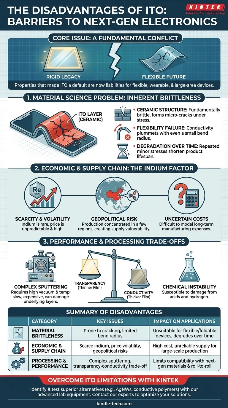
While indispensable in modern electronics, Indium Tin Oxide (ITO) is defined by a significant set of disadvantages. Its primary drawbacks stem from the scarcity and cost of indium, its inherent brittleness which makes it unsuitable for flexible applications, and complex manufacturing processes that limit its use in next-generation devices.
The core issue with ITO is a fundamental conflict: the very properties that made it the default transparent conductor for decades are now becoming major liabilities. Its brittleness, cost, and processing demands are significant barriers for the future of flexible, wearable, and large-area electronics.
The Material Science Problem: Inherent Brittleness
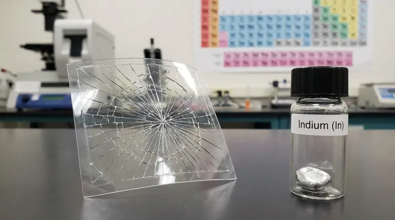
ITO is a ceramic material, and like most ceramics, it is fundamentally brittle. This single characteristic is its most significant technical weakness in the context of modern device requirements.
Why ITO Cracks
As a sputtered thin film, ITO has an amorphous or polycrystalline structure. When subjected to mechanical stress—especially bending, folding, or stretching—this structure does not yield gracefully.
Instead, micro-cracks form and quickly propagate. This failure mode is catastrophic for electrical performance.
The Impact on Flexible Devices
The push toward flexible displays, foldable phones, and wearable sensors exposes this weakness directly. ITO films can only withstand a very small bend radius before their conductivity plummets.
A single fold can increase the material's sheet resistance (a measure of conductivity) by several orders of magnitude, rendering the device useless. This makes it a poor choice for any truly dynamic or flexible application.
Performance Degradation Over Time
Even in applications that aren't meant to be actively flexed, repeated minor stresses, vibrations, or thermal cycling can lead to the formation of micro-cracks over time. This results in device degradation and reduced product lifetime.
The Economic and Supply Chain Problem: The Indium Factor
Beyond its physical limitations, the reliance on indium creates significant economic and geopolitical risks.
Scarcity and Price Volatility
Indium is not an abundant element. It is most often sourced as a byproduct of zinc mining, meaning its supply is tied to the demand for another metal.
This limited supply chain makes its price highly volatile and subject to dramatic spikes, introducing significant uncertainty into manufacturing cost models.
Geopolitical Supply Risk
A vast majority of the world's indium production is concentrated in a few countries, primarily China. This creates a supply chain vulnerability for companies and countries reliant on it for critical technology manufacturing.
Any trade dispute, policy change, or mining disruption can have an immediate and severe impact on the global availability and cost of ITO.
Understanding the Performance and Processing Trade-offs
Manufacturing and integrating ITO into a device is a complex process filled with compromises that affect performance and cost.
The Transparency vs. Conductivity Dilemma
There is a direct trade-off between ITO's electrical conductivity and its optical transparency. To achieve lower resistance (better conductivity), you need a thicker film.
However, thicker films are less transparent and can have a noticeable yellowish tint, which is undesirable in high-quality displays. They also absorb more light in the blue and UV spectrum, affecting color accuracy and efficiency in devices like OLEDs.
The Constraints of Sputtering
The most common method for depositing ITO is magnetron sputtering, a physical vapor deposition (PVD) technique. This process requires a high vacuum and often elevated temperatures.
These conditions are expensive to create and maintain, are relatively slow, and can damage sensitive underlying layers, such as the organic materials used in OLEDs or perovskite solar cells. This limits its compatibility with certain next-generation materials and roll-to-roll manufacturing.
Chemical Instability
While relatively stable, ITO can be damaged by strong acids and is known to degrade in the presence of hydrogen. This requires careful consideration during multi-step fabrication processes where other layers are patterned or deposited.
Making the Right Choice for Your Application
Choosing a transparent conductor requires weighing the well-understood benefits of ITO against its significant and growing list of drawbacks. The right choice depends entirely on your product's core requirements.
- If your primary focus is a rigid, high-resolution display (like a standard smartphone or monitor): ITO remains a viable, albeit expensive, choice because its performance is proven and its brittleness is not a factor.
- If your primary focus is a flexible, foldable, or wearable device: ITO is a fundamentally poor choice. You should prioritize alternatives like silver nanowires (AgNWs), metal mesh, or conductive polymers.
- If your primary focus is a low-cost, large-area application (like smart windows or some solar panels): The high cost of indium and the batch-processing nature of sputtering make ITO less competitive. Solution-processable alternatives may offer a better cost-to-performance ratio.
Understanding these limitations is the first step toward innovating beyond them and selecting the right material for the future.
Summary Table:
| Disadvantage Category | Key Issues | Impact on Applications |
|---|---|---|
| Material Brittleness | Prone to cracking under stress, limited bend radius | Unsuitable for flexible/foldable devices, degrades over time |
| Economic & Supply Chain | Scarce indium, price volatility, geopolitical risks | High cost, unreliable supply for large-scale production |
| Processing & Performance | Complex sputtering, transparency-conductivity trade-off | Limits compatibility with next-gen materials and roll-to-roll manufacturing |
Struggling with ITO's limitations for your flexible or cost-sensitive project? KINTEK specializes in advanced lab equipment and materials for electronics R&D. Our experts can help you identify and test superior alternatives like silver nanowires or conductive polymers tailored to your specific needs. Contact our team today to optimize your transparent conductor solutions and enhance your product's performance and durability.
Visual Guide
Related Products
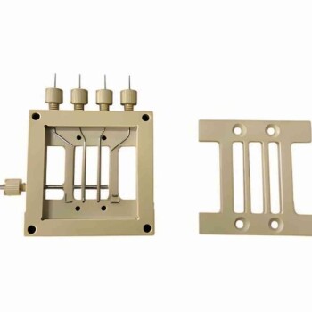
- Side Window Optical Electrolytic Electrochemical Cell
- Custom Ion Conductivity Test Fixtures for Fuel Cell Research
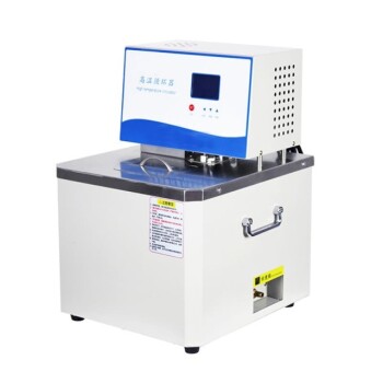
- 5L Heating Chilling Circulator Cooling Water Bath Circulator for High and Low Temperature Constant Temperature Reaction
- 10L Heating Chilling Circulator Cooling Water Bath Circulator for High and Low Temperature Constant Temperature Reaction
- Reference Electrode Calomel Silver Chloride Mercury Sulfate for Laboratory Use
People Also Ask
- What are the key operational procedures during an experiment with a side-window optical electrolytic cell? Ensure Accurate, Bubble-Free Measurements
- What is the correct procedure for post-experiment shutdown and cleaning of a side-window optical electrolytic cell? Ensure Safety and Data Accuracy
- What are the typical specifications for the volume and apertures of a side-window optical electrolytic cell? Key Specs for Your Spectroelectrochemistry
- What is a side-window optical electrolytic cell? See Your Electrochemical Reactions in Action
- What maintenance procedures are recommended for a side-window optical electrolytic cell? Ensure Data Accuracy & Extend Cell Lifespan