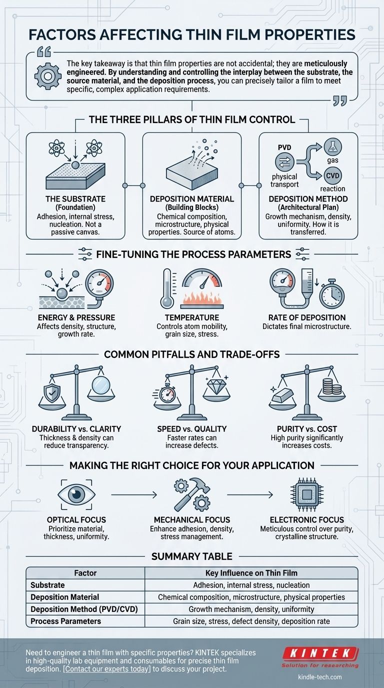
At its core, the final properties of a thin film are determined by three fundamental factors: the substrate it is placed on, the material being deposited, and the specific deposition method and parameters used to create it. These elements interact to control everything from the film's durability and transparency to its electrical conductivity.
The key takeaway is that thin film properties are not accidental; they are meticulously engineered. By understanding and controlling the interplay between the substrate, the source material, and the deposition process, you can precisely tailor a film to meet specific, complex application requirements.
The Three Pillars of Thin Film Control
Every thin film is the result of a carefully controlled process. The final outcome is dictated by a set of foundational choices that influence the film's structure at the atomic level.
1. The Substrate: The Foundation of the Film
The substrate is the surface upon which the film is grown, and its properties are critical. It is not a passive canvas.
The chemical nature and topography of the substrate directly influence how the first layers of the film form, a process known as nucleation. A film's adhesion and internal stress are heavily dependent on the binding energy between the substrate and the deposited material.
2. The Deposition Material: The Building Blocks
The choice of target material fundamentally defines the potential properties of the film. This material is the source from which atoms or molecules are transferred to the substrate.
Whether you are using sputtering, evaporation, or chemical vapor deposition, the composition of this source material directly dictates the film's final chemical composition, microstructure, and physical properties.
3. The Deposition Method: The Architectural Plan
The technique used to deposit the film is arguably the most influential factor, as it controls how the material is transferred and assembled on the substrate.
The two primary families of deposition are Physical Vapor Deposition (PVD) and Chemical Vapor Deposition (CVD). PVD methods, like sputtering, physically transport atoms from a target to the substrate. CVD uses precursor gases that react on the substrate surface to form the film.
The choice between these methods is determined by the desired film properties, thickness, and the nature of the substrate itself.
Fine-Tuning the Process Parameters
Within any chosen deposition method, a set of process parameters acts as fine-tuning knobs. These variables allow for precise control over the film's growth and final characteristics.
The Role of Energy and Pressure
The energy of the impinging species (the atoms arriving at the substrate) and the working pressure of the chamber significantly affect the film's density and structure. Higher energy can lead to denser, more durable films, while pressure can influence the growth rate and uniformity.
The Impact of Temperature
Substrate temperature is a critical parameter that controls the mobility of atoms once they land on the surface. Adjusting the temperature influences the film's grain size, crystalline structure, and internal stress, which in turn affects its mechanical and optical properties.
The Rate of Deposition
The impingement rate, or how quickly material is deposited, also plays a crucial role. This rate, in combination with temperature and pressure, dictates the final microstructure of the film.
Common Pitfalls and Trade-offs
Achieving a specific thin film property often involves balancing competing factors. It is rare to optimize one characteristic without affecting another.
Durability vs. Optical Clarity
Increasing a film's mechanical durability or scratch resistance often requires a denser, thicker film. However, increasing thickness or density can negatively impact optical transparency or introduce unwanted stress, altering its performance in photonic applications.
Deposition Speed vs. Film Quality
A faster deposition rate might be desirable for manufacturing efficiency, but it can lead to a more disordered or porous film structure. Slower, more controlled deposition generally yields higher-quality films with superior uniformity and fewer defects, but at a higher cost and longer processing time.
Material Purity vs. Cost
While a high-purity target material is essential for achieving predictable electronic or optical properties, it can significantly increase costs. For less sensitive mechanical or decorative applications, a lower-purity material may be a perfectly acceptable and cost-effective compromise.
Making the Right Choice for Your Application
Ultimately, the factors you prioritize depend entirely on the intended use of the thin film. Your application's requirements should guide every decision in the deposition process.
- If your primary focus is optical performance: Prioritize the selection of the deposition material and precise control over film thickness and uniformity.
- If your primary focus is mechanical durability: Concentrate on enhancing substrate adhesion, increasing film density through energetic deposition, and managing internal stress via temperature control.
- If your primary focus is electronic properties: The purity of the target material and meticulous control over the film's crystalline microstructure are the most critical factors.
By systematically controlling these core factors, you can engineer thin films to meet even the most demanding performance criteria.
Summary Table:
| Factor | Key Influence on Thin Film |
|---|---|
| Substrate | Adhesion, internal stress, nucleation |
| Deposition Material | Chemical composition, microstructure, physical properties |
| Deposition Method (PVD/CVD) | Growth mechanism, density, uniformity |
| Process Parameters | Grain size, stress, defect density, deposition rate |
Need to engineer a thin film with specific properties?
The right equipment is fundamental to controlling the factors discussed in this article. KINTEK specializes in high-quality lab equipment and consumables for precise thin film deposition. Whether your application demands superior optical clarity, mechanical durability, or specific electronic properties, our solutions help you achieve consistent, reliable results.
Contact our experts today to discuss your project requirements and discover how KINTEK can support your laboratory's thin film innovation.
Visual Guide
Related Products
- Aluminized Ceramic Evaporation Boat for Thin Film Deposition
- Tungsten Evaporation Boat for Thin Film Deposition
- Electron Beam Evaporation Coating Oxygen-Free Copper Crucible and Evaporation Boat
- Molybdenum Tungsten Tantalum Evaporation Boat for High Temperature Applications
- Vacuum Hot Press Furnace Machine for Lamination and Heating
People Also Ask
- What is the widely used boat made of in thermal evaporation? Choosing the Right Material for High-Purity Deposition
- What is thin film deposition? Unlock Advanced Surface Engineering for Your Materials
- What are thin films deposited by evaporation? A Guide to High-Purity Coating
- What is the source of evaporation for thin film? Choosing Between Thermal and E-Beam Methods
- What are the alternatives to sputtering? Choose the Right Thin Film Deposition Method


