The most common method for transferring graphene involves using a polymer support layer, typically PMMA, to move the single-atom-thick film from its growth substrate to a target substrate. After coating the graphene with PMMA, the original growth substrate is chemically etched away, leaving a floating PMMA/graphene film that can be carefully placed onto a new surface before the PMMA is dissolved.
The core challenge of graphene transfer is moving a fragile, one-atom-thick sheet from one surface to another without introducing wrinkles, tears, or chemical contamination that would degrade its exceptional properties.
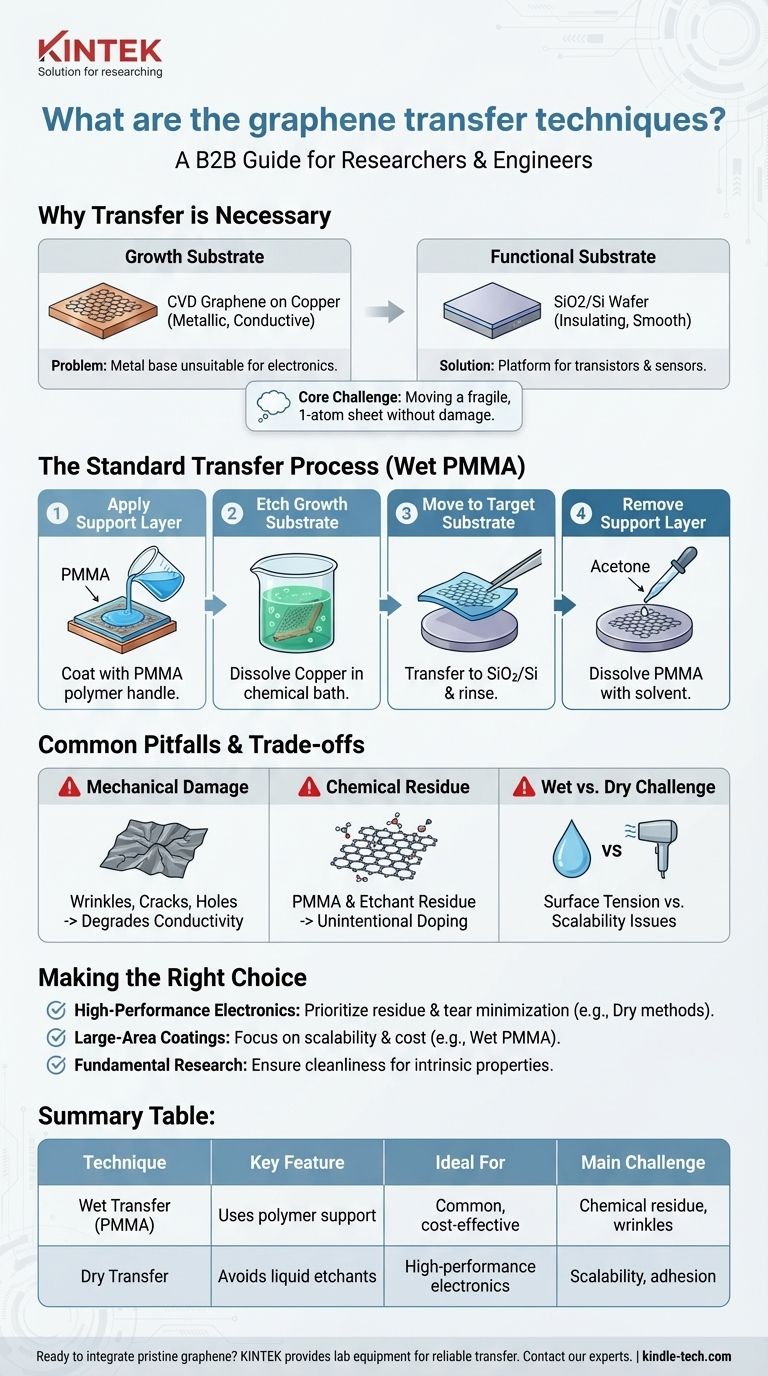
Why Graphene Transfer is Necessary
The Problem of the Growth Substrate
Graphene is often synthesized using methods like Chemical Vapor Deposition (CVD), where it grows as a thin film on a metallic catalyst, such as copper foil.
While excellent for growth, these metallic substrates are not suitable for the final applications of graphene, particularly in electronics where an insulating or semiconducting base is required.
Moving to a Functional Substrate
To build transistors, sensors, or other devices, the graphene must be moved to a functional target substrate.
A silicon wafer with an oxide layer (SiO2/Si) is a common choice because it is insulating, has a very smooth surface, and is the standard platform for the entire semiconductor industry. The transfer process is the critical bridge between graphene synthesis and its practical application.
The Anatomy of a Standard Transfer Process
The most established technique is a "wet transfer" that uses a polymer scaffold to support the graphene film.
Step 1: Applying the Support Layer
A polymer solution, most commonly poly(methyl methacrylate) or PMMA, is coated directly on top of the graphene film as it sits on its original growth substrate.
This PMMA layer acts as a temporary handle and mechanical support, preventing the ultrathin graphene from folding, tearing, or disintegrating during subsequent steps.
Step 2: Etching the Growth Substrate
The entire sample (PMMA/graphene/copper) is placed in a chemical bath, or etchant, that selectively dissolves the original growth substrate.
For a copper substrate, an etchant like ferric chloride or ammonium persulfate is used. This process leaves the PMMA/graphene film floating on the surface of the liquid.
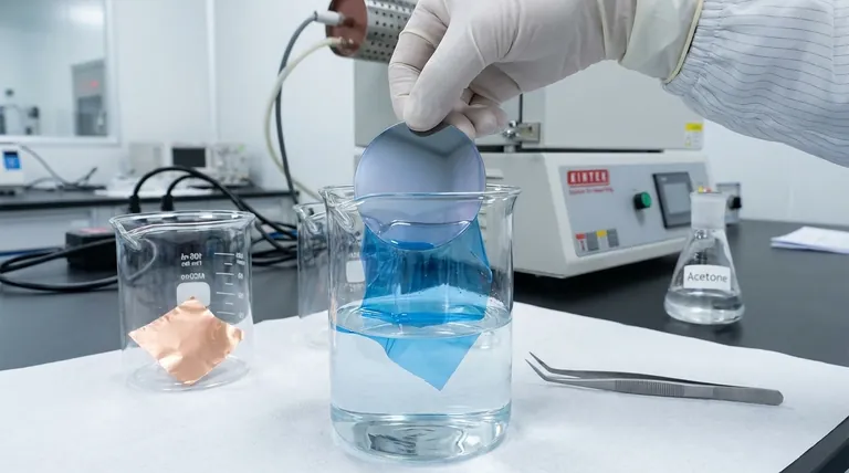
Step 3: Moving to the Target Substrate
The floating film is carefully "fished" out of the etchant solution, often by submerging the target SiO2/Si substrate beneath it and slowly lifting it out.
The film is then rinsed in deionized water to remove residual etchant before being carefully draped over the new substrate.
Step 4: Removing the Support Layer
Once the film is securely positioned on the target substrate, the final step is to remove the PMMA support layer.
This is typically done by dissolving the PMMA with a solvent like acetone, followed by a final rinse. If successful, only a clean, single layer of graphene remains on the new substrate.
Common Pitfalls and Trade-offs
A perfect transfer is the ideal, but the reality involves significant challenges that can impact the quality of the final graphene film.
The Problem of Mechanical Damage
Handling an atom-thick sheet is incredibly difficult. Wrinkles, cracks, and holes are common defects introduced during the transfer.
These imperfections disrupt the continuous honeycomb lattice of the graphene, degrading its electrical conductivity and mechanical strength.
The Issue of Chemical Residue
The chemicals used in the process—namely the PMMA and the etchants—can leave behind residue and contamination.
Even trace amounts of polymer or metallic ions can unintentionally "dope" the graphene, altering its electronic properties and hindering device performance.
The Wet vs. Dry Challenge
The standard "wet" transfer process described introduces surface tension from liquids, which can cause wrinkling and require careful drying.
This has led to the development of alternative "dry" transfer methods, though they often have their own trade-offs regarding scalability and film adhesion. The wet PMMA method remains the most common due to its relative simplicity and low cost.
Making the Right Choice for Your Goal
The acceptable level of defects in a transfer process depends entirely on the intended application.
- If your primary focus is high-performance electronics: The priority must be a transfer process that minimizes chemical residue and mechanical tears, as these directly impact carrier mobility and device reliability.
- If your primary focus is large-area coatings or composites: Scalability, cost, and maintaining film continuity over large areas are more critical than achieving a perfectly pristine, defect-free monolayer.
- If your primary focus is fundamental research: The cleanliness of the transfer and the choice of substrate are paramount to ensure that experimental measurements reflect the intrinsic properties of graphene, not artifacts from the process.
Ultimately, mastering the transfer of graphene is just as crucial as mastering its growth for unlocking its true potential.
Summary Table:
| Technique | Key Feature | Ideal For | Main Challenge |
|---|---|---|---|
| Wet Transfer (PMMA) | Uses polymer support layer | Common method, cost-effective | Chemical residue, wrinkles |
| Dry Transfer | Avoids liquid etchants | High-performance electronics | Scalability, adhesion |
Ready to integrate pristine graphene into your devices? The right transfer technique is critical for performance. KINTEK specializes in providing the lab equipment and consumables necessary for reliable graphene transfer, serving research and development laboratories. Contact our experts today to discuss how we can support your specific application needs and ensure high-quality results.
Visual Guide
Related Products
- High Purity Pure Graphite Crucible for Evaporation
- Graphite Disc Rod and Sheet Electrode Electrochemical Graphite Electrode
People Also Ask
- Why is a high-purity graphite crucible required for FLiNaK molten salts? Ensure Purity & Data Integrity
- Is graphite used to make heat resistant crucibles? Unlock Faster Melting and Superior Performance
- Why is a high-purity graphite crucible ideal for nitrogen-doped graphene at 1500 °C? Maximize Purity and Stability
- What are the advantages of using graphite crucibles in 3000°C experiments? Achieve Superior Purity and Performance
- Why is a high-purity graphite crucible required for Chromel-TaC composites? Ensure Peak Purity at 1400°C