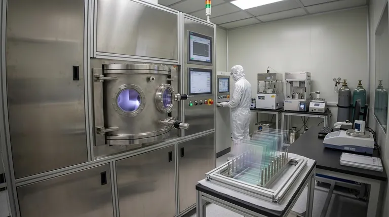
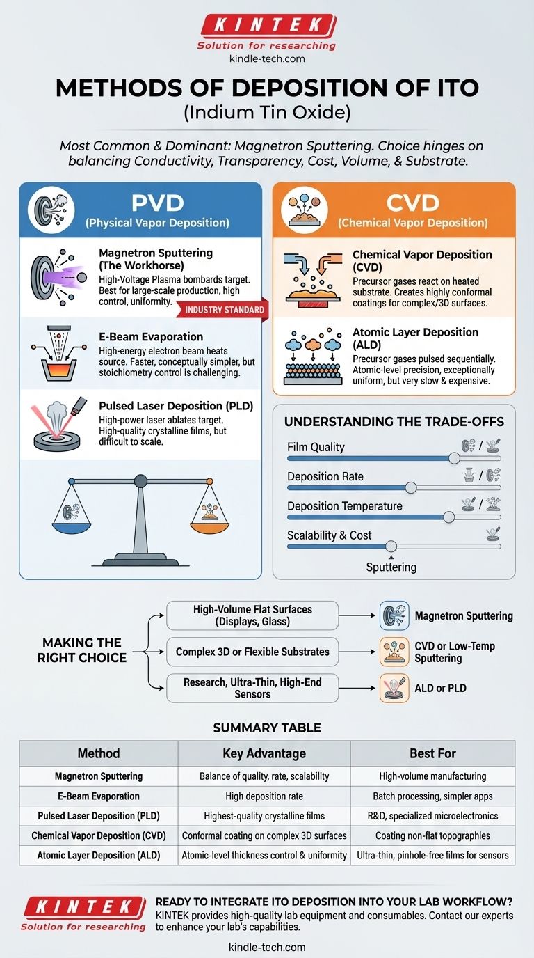
For depositing Indium Tin Oxide (ITO), the most common and industrially dominant method is magnetron sputtering. While other techniques like evaporation, chemical vapor deposition (CVD), and atomic layer deposition (ALD) are also used, sputtering provides the best balance of film quality, deposition rate, and scalability for the majority of commercial applications, such as displays and touch screens.
Choosing a deposition method for ITO is not about finding a single "best" technique, but about understanding a critical set of trade-offs. The decision hinges on balancing your specific requirements for electrical conductivity, optical transparency, cost, production volume, and substrate type.
The Two Pillars of Deposition: PVD and CVD
Nearly all ITO deposition techniques fall into two main categories: Physical Vapor Deposition (PVD) and Chemical Vapor Deposition (CVD). Understanding this distinction is the first step to selecting the right method.
PVD methods use physical processes—like impact or heating—to transform a solid ITO target into a vapor, which then condenses onto a substrate in a vacuum. CVD methods use chemical reactions between precursor gases to form the solid ITO film on the substrate surface.
Physical Vapor Deposition (PVD): The Industry Standard
PVD is favored for its ability to produce high-purity, dense films with excellent properties.
Magnetron Sputtering (The Workhorse) This is the go-to method for large-scale production of ITO-coated glass and plastic. A high-voltage plasma is used to bombard a ceramic ITO target, ejecting atoms that deposit onto the substrate.
Its dominance comes from its high degree of control over film thickness, uniformity over large areas, and the excellent optoelectronic properties of the resulting film.
Electron-Beam (E-Beam) Evaporation In this method, a high-energy electron beam heats and evaporates ITO source material from a crucible in a vacuum. The vapor then travels in a line-of-sight path and condenses on the substrate.
While often faster and conceptually simpler than sputtering, controlling the precise stoichiometry (the Indium-to-Tin ratio) can be challenging, which directly impacts the film's performance.
Pulsed Laser Deposition (PLD) PLD uses a high-power laser to ablate a rotating ITO target, creating a plasma plume that deposits a film on the substrate.
This method is primarily used in research and development for creating very high-quality, crystalline films. However, it is difficult to scale for large-area production, making it impractical for most commercial uses.
Chemical Vapor Deposition (CVD): For Precision and Conformality
CVD builds films from the ground up through chemical reactions, offering unique advantages for specific applications.
Chemical Vapor Deposition (CVD) In a CVD process, volatile precursor gases containing indium, tin, and oxygen are introduced into a reaction chamber. They react at the surface of a heated substrate to form a solid ITO film.
The key advantage of CVD is its ability to create highly conformal coatings that uniformly cover complex, non-flat, or 3D surfaces where line-of-sight PVD methods would fail.
Atomic Layer Deposition (ALD) ALD is a sophisticated subtype of CVD where precursor gases are pulsed into the chamber one at a time. This enables the film to be grown with atomic-level precision, one monolayer at a time.
This technique provides unparalleled control over thickness and creates exceptionally uniform, pinhole-free films. Its primary drawback is that it is an extremely slow and expensive process, reserving it for highly specialized, high-value applications.
Understanding the Trade-offs
No single method is perfect for every scenario. The right choice depends entirely on your project's priorities.
Film Quality vs. Deposition Rate
Sputtering offers a superb balance, producing high-quality films at commercially viable rates. PLD can produce the highest-quality crystalline films but is very slow. Evaporation is fast but can compromise film quality and repeatability.
ALD provides the highest conformity and thickness control but has the slowest deposition rate of all, measured in nanometers per hour.
Deposition Temperature
The substrate you are coating is a critical factor. CVD processes often require high substrate temperatures, which can damage sensitive materials like flexible polymers or plastics.
Many PVD processes, especially sputtering, can be performed at or near room temperature, making them ideal for temperature-sensitive applications like flexible electronics.
Scalability and Cost
For mass production of flat substrates (e.g., displays, solar panels, architectural glass), magnetron sputtering is the undisputed leader due to its scalability and mature ecosystem.
CVD can also be scaled for high-volume production, but the equipment and precursor gas costs can be higher. E-beam evaporation is often a lower-cost option for batch processing, while PLD and ALD are typically the most expensive and reserved for R&D or niche products.
Making the Right Choice for Your Application
Your application's end goal dictates the optimal deposition method.
- If your primary focus is high-volume manufacturing of flat surfaces like displays or smart glass: Magnetron sputtering is the industry standard for its balance of quality, rate, and cost-effectiveness.
- If your primary focus is coating complex 3D topographies or flexible substrates: CVD or low-temperature sputtering are your best options for achieving conformal coverage without damaging the substrate.
- If your primary focus is research or creating ultra-thin, perfect films for high-end sensors or microelectronics: ALD or PLD provide the ultimate precision and film quality, justifying their higher cost and slower speed.
Understanding these core trade-offs empowers you to select the deposition technique that aligns perfectly with your material, performance, and production goals.
Summary Table:
| Method | Category | Key Advantage | Best For |
|---|---|---|---|
| Magnetron Sputtering | PVD | Balance of quality, rate, and scalability | High-volume manufacturing (displays, glass) |
| E-Beam Evaporation | PVD | High deposition rate | Batch processing, simpler applications |
| Pulsed Laser Deposition (PLD) | PVD | Highest-quality crystalline films | R&D, specialized microelectronics |
| Chemical Vapor Deposition (CVD) | CVD | Conformal coating on complex 3D surfaces | Coating non-flat topographies |
| Atomic Layer Deposition (ALD) | CVD | Atomic-level thickness control & uniformity | Ultra-thin, pinhole-free films for sensors |
Ready to Integrate ITO Deposition into Your Lab Workflow?
Choosing the right deposition technique is critical for your project's success. KINTEK specializes in providing high-quality lab equipment and consumables for advanced material deposition processes. Whether you are scaling up production or pushing the boundaries of research, our expertise can help you achieve optimal film quality and performance.
Contact our experts today to discuss your specific ITO deposition needs and discover how KINTEK's solutions can enhance your laboratory's capabilities and efficiency.
Visual Guide
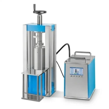
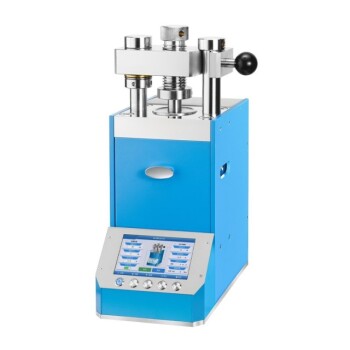
Related Products
- Chemical Vapor Deposition CVD Equipment System Chamber Slide PECVD Tube Furnace with Liquid Gasifier PECVD Machine
- HFCVD Machine System Equipment for Drawing Die Nano-Diamond Coating
- Customer Made Versatile CVD Tube Furnace Chemical Vapor Deposition Chamber System Equipment
- Inclined Rotary Plasma Enhanced Chemical Vapor Deposition PECVD Equipment Tube Furnace Machine
- Inclined Rotary Plasma Enhanced Chemical Vapor Deposition PECVD Equipment Tube Furnace Machine
People Also Ask
- What is the chemical vapor deposition growth process? Build Superior Thin Films from the Atom Up
- What are the advantages of chemical vapor deposition? Achieve Superior Thin Films for Your Lab
- What are the processes of vapor phase deposition? Understand CVD vs. PVD for Superior Thin Films
- What types of substrates are used in CVD to facilitate graphene films? Optimize Graphene Growth with the Right Catalyst
- What are the core advantages of PE-CVD in OLED encapsulation? Protect Sensitive Layers with Low-Temp Film Deposition