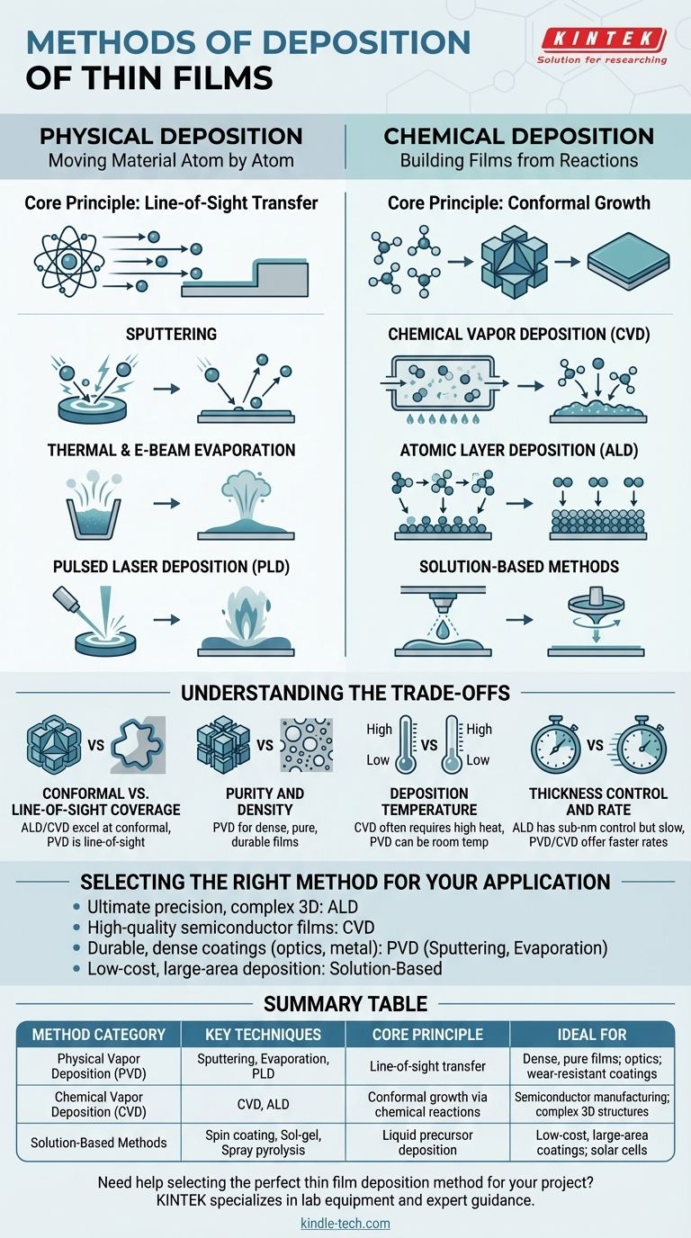
The primary methods for depositing thin films fall into two main categories: Physical Deposition and Chemical Deposition. Physical methods, like sputtering or evaporation, involve physically transferring material from a source to a substrate, while chemical methods, like Chemical Vapor Deposition (CVD), use chemical reactions to create the film directly on the substrate's surface.
The choice between deposition techniques is not about finding the "best" method, but about understanding a fundamental trade-off. Physical methods offer versatility and high-purity films, while chemical methods provide unparalleled conformity and precision for coating complex structures.
Physical Deposition: Moving Material Atom by Atom
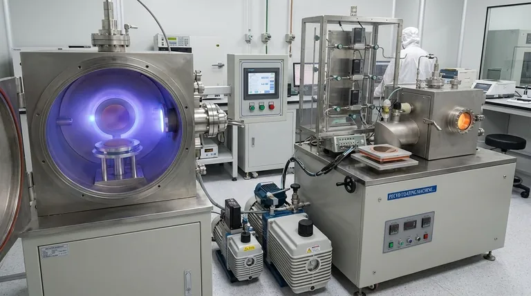
Physical Vapor Deposition (PVD) encompasses a family of techniques where a material is converted into a vapor phase in a vacuum and then condensed onto a substrate to form a thin film. This process is like a microscopic spray painting, but with atoms or molecules.
The Core Principle: Line-of-Sight Transfer
In most PVD processes, the vaporized material travels in a straight line from the source to the substrate. This is known as line-of-sight deposition.
Sputtering
Sputtering uses energetic ions, typically from a plasma, to bombard a source material known as a "target." This collision ejects atoms from the target, which then travel and deposit onto the substrate. Magnetron sputtering is a common enhancement that uses magnetic fields to increase efficiency.
Thermal & E-Beam Evaporation
These methods involve heating a source material in a high vacuum until it evaporates. The resulting vapor travels and condenses on a cooler substrate. Thermal evaporation uses resistive heating, while electron beam (e-beam) evaporation uses a high-energy beam of electrons to melt and evaporate the source.
Pulsed Laser Deposition (PLD)
In PLD, a high-power pulsed laser is focused on a target. The intense energy ablates (blasts off) material from the target, creating a plasma plume that expands and deposits a thin film onto a nearby substrate.
Chemical Deposition: Building Films from Reactions
Chemical deposition methods create a solid film on a substrate through a chemical reaction. The atoms for the film are delivered by precursor molecules, which can be in a gas or liquid phase.
The Core Principle: Conformal Growth
Because these methods rely on chemical reactions that can occur on all exposed surfaces, they are excellent for creating conformal coatings. This means they can uniformly coat complex, three-dimensional structures without the shadowing effects seen in line-of-sight PVD.
Chemical Vapor Deposition (CVD)
CVD is a cornerstone of the semiconductor industry. Precursor gases are introduced into a reaction chamber, where they decompose and react on a heated substrate to form the desired film. Its high precision makes it ideal for manufacturing integrated circuits.
Atomic Layer Deposition (ALD)
ALD is a subtype of CVD that offers the ultimate level of thickness control. It uses sequential, self-limiting chemical reactions to deposit a film one single atomic layer at a time. This provides perfect conformity and precise thickness control down to the angstrom level.
Solution-Based (Liquid Phase) Methods
These low-cost methods use a liquid chemical precursor. Techniques include spin coating, where a substrate is spun at high speed to spread a liquid film; sol-gel, which uses a chemical solution to form a gel-like network; and spray pyrolysis, where a solution is sprayed onto a hot substrate to induce a chemical reaction.
Understanding the Trade-offs
Choosing the right deposition method requires balancing several key factors. There is no single best technique; the optimal choice depends entirely on the application's requirements.
Conformal vs. Line-of-Sight Coverage
Chemical methods like CVD and ALD excel at conformal coverage, uniformly coating trenches, holes, and complex 3D objects. PVD methods are primarily line-of-sight and struggle to coat hidden surfaces or deep features.
Purity and Density
PVD techniques, particularly sputtering, are renowned for producing very dense, pure, and durable films. This makes them ideal for optical coatings, protective layers on tools, and metallic interconnects in electronics.
Deposition Temperature
CVD processes often require high substrate temperatures to drive the necessary chemical reactions. This can be a limitation for temperature-sensitive substrates. Many PVD processes can be performed at or near room temperature.
Thickness Control and Rate
ALD offers unparalleled, sub-nanometer thickness control but is a very slow process. CVD and PVD provide a good balance of excellent control (through time and monitoring) and much faster deposition rates suitable for manufacturing.
Selecting the Right Method for Your Application
Your final choice depends on balancing performance, cost, and the specific properties your film requires.
- If your primary focus is ultimate precision and perfect conformal coating on complex 3D structures: ALD is the definitive choice, despite its slow speed.
- If your primary focus is high-quality, high-purity films for semiconductor manufacturing: CVD is the industry standard due to its precision, purity, and established process reliability.
- If your primary focus is a durable, dense coating for optics, wear resistance, or metal layers: PVD methods like sputtering and e-beam evaporation offer unmatched performance and versatility.
- If your primary focus is low-cost, large-area deposition for applications like solar cells or simple electronics: Solution-based methods like spin coating or spray pyrolysis provide a scalable and cost-effective path.
Understanding these fundamental deposition principles empowers you to select the precise tool needed to engineer materials from the atoms up.
Summary Table:
| Method Category | Key Techniques | Core Principle | Ideal For |
|---|---|---|---|
| Physical Vapor Deposition (PVD) | Sputtering, Evaporation, PLD | Line-of-sight transfer | Dense, pure films; optics; wear-resistant coatings |
| Chemical Vapor Deposition (CVD) | CVD, ALD | Conformal growth via chemical reactions | Semiconductor manufacturing; complex 3D structures |
| Solution-Based Methods | Spin coating, Sol-gel, Spray pyrolysis | Liquid precursor deposition | Low-cost, large-area coatings; solar cells |
Need help selecting the perfect thin film deposition method for your project? KINTEK specializes in lab equipment and consumables, serving laboratory needs with expert guidance on PVD, CVD, and ALD systems. Let our team help you achieve precise, high-quality films tailored to your application—whether for semiconductors, optics, or research. Contact us today to discuss your specific requirements and discover how KINTEK can enhance your thin film deposition process!
Visual Guide
Related Products
- Aluminized Ceramic Evaporation Boat for Thin Film Deposition
- Tungsten Evaporation Boat for Thin Film Deposition
- Electron Beam Evaporation Coating Oxygen-Free Copper Crucible and Evaporation Boat
- Molybdenum Tungsten Tantalum Evaporation Boat for High Temperature Applications
- HFCVD Machine System Equipment for Drawing Die Nano-Diamond Coating
People Also Ask
- What is thin film deposition? Unlock Advanced Surface Engineering for Your Materials
- What are thin films deposited by evaporation? A Guide to High-Purity Coating
- What is the chemical method for thin film deposition? Build Films from the Molecular Level Up
- Why are high-purity ceramic boats used for lignin activation? Ensure Purity & Thermal Stability
- What is the widely used boat made of in thermal evaporation? Choosing the Right Material for High-Purity Deposition


