At its core, Chemical Vapor Deposition (CVD) is a sophisticated process for building a solid material from a gas. The fundamental steps involve introducing reactive precursor gases into a controlled chamber, energizing them to induce a chemical reaction, and allowing that reaction to form a solid thin film on a target surface, known as a substrate. All remaining gaseous byproducts are then exhausted from the chamber.
The central principle of CVD is not merely coating a surface, but rather synthesizing a new material directly onto it. It leverages controlled chemical reactions in a vapor phase to construct a high-purity, solid film, offering precise control over the final material's structure and composition.
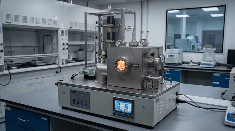
The Essential Components of a CVD System
Before the process can begin, a few key components must be in place. Each plays a critical role in the final outcome of the deposition.
The Precursor Gases (The Building Blocks)
Precursors are volatile gases that contain the specific atoms or molecules needed for the desired film. For example, to create a silicon film, a precursor like silane gas (SiH₄) might be used.
These gases act as the transport mechanism, carrying the essential elements into the reaction chamber in a controlled, gaseous state.
The Substrate (The Foundation)
The substrate is the material onto which the thin film is grown. It is often heated to provide the thermal energy needed to drive the chemical reactions.
In some cases, like the growth of graphene on copper foil, the substrate also acts as a catalyst, actively participating in the reaction to facilitate the decomposition of the precursor and provide a surface for the new material to form.
The Reaction Chamber (The Controlled Environment)
The entire process takes place inside a sealed chamber. This allows for precise control over critical variables like temperature, pressure, and gas composition.
This controlled environment is essential for ensuring the reaction happens as intended, leading to a film with the desired purity and structural properties.
A Step-by-Step Breakdown of the Deposition Process
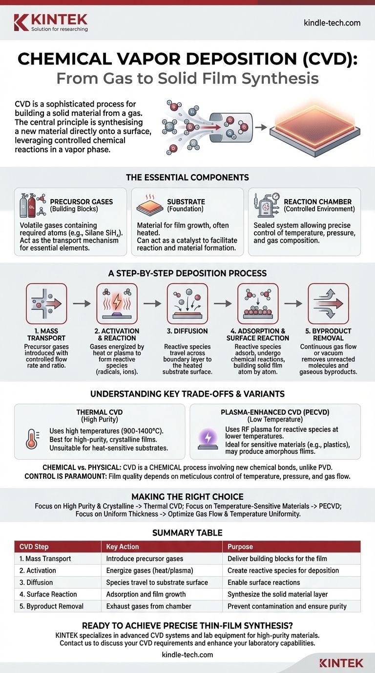
The CVD process can be understood as a sequence of five distinct physical and chemical events.
Step 1: Mass Transport into the Chamber
The process begins by introducing one or more precursor gases into the reaction chamber. Their flow rate and ratio are carefully controlled to manage the growth rate and composition of the final film.
Step 2: Activation and Gas-Phase Reactions
The gases are energized, typically through heat or plasma. This activation breaks down the stable precursor molecules into more reactive species, such as radicals or ions.
Sometimes, preliminary chemical reactions can occur between these species in the gas phase before they ever reach the substrate.
Step 3: Diffusion to the Substrate Surface
These newly formed reactive species then travel or diffuse from the main gas flow across a boundary layer to reach the surface of the heated substrate.
Step 4: Adsorption and Surface Reaction
This is the critical deposition step. The reactive species land on the substrate surface (adsorption) and undergo further chemical reactions.
These surface reactions are what build the solid film, atom by atom or molecule by molecule. The byproducts of this reaction are then released from the surface back into the gas phase.
Step 5: Byproduct Removal
Finally, a continuous gas flow through the chamber, or a vacuum system, removes all the unreacted precursor molecules and the gaseous byproducts from the reaction chamber. This prevents them from contaminating the film and clears the way for fresh reactants.
Understanding the Trade-offs and Key Variants
While the steps are consistent, the conditions under which they occur create important distinctions and trade-offs.
Thermal CVD vs. Plasma-Enhanced CVD (PECVD)
The energy source is a primary differentiator. Traditional thermal CVD uses high temperatures (often 900-1400 °C) to break down the precursors. This produces very high-purity, often crystalline films, but is unsuitable for substrates that cannot withstand the heat.
Plasma-Enhanced CVD (PECVD) uses an RF plasma to create reactive radicals at much lower temperatures. This allows for deposition on sensitive materials like plastics but may result in a different film structure, often amorphous rather than crystalline.
Chemical Reactions vs. Physical Processes
It is crucial to understand that CVD is a chemical process. The film is the product of new chemical bonds forming on the substrate.
This distinguishes it from Physical Vapor Deposition (PVD), which relies on physical mechanisms like evaporation or sputtering to transfer material from a solid source to the substrate without a fundamental chemical reaction.
The Importance of Control
The quality of the final film—its thickness, uniformity, purity, and structure—is directly dependent on meticulous control over every step. Minor fluctuations in temperature, pressure, or gas flow can have significant impacts on the final material.
Making the Right Choice for Your Goal
Understanding these steps allows you to see how the CVD process can be tuned for specific outcomes.
- If your primary focus is creating highly pure, crystalline films (like for semiconductors or graphene): You will likely rely on high-temperature thermal CVD, where precise temperature control and the right catalytic substrate are paramount.
- If your primary focus is coating a temperature-sensitive material (like a polymer or a finished device): Your best option is a lower-temperature method like PECVD, which uses plasma energy instead of intense heat to drive the reaction.
- If your primary focus is achieving perfectly uniform thickness over a large area: You must prioritize optimizing the gas flow dynamics and ensuring absolute temperature uniformity across the entire substrate.
Ultimately, mastering the CVD process is about precisely controlling a sequence of chemical events to build materials from the atom up.
Summary Table:
| CVD Step | Key Action | Purpose |
|---|---|---|
| 1. Mass Transport | Introduce precursor gases into chamber | Deliver building blocks for the film |
| 2. Activation | Energize gases (heat/plasma) | Create reactive species for deposition |
| 3. Diffusion | Species travel to substrate surface | Enable surface reactions |
| 4. Surface Reaction | Adsorption and film growth on substrate | Synthesize the solid material layer |
| 5. Byproduct Removal | Exhaust gases from chamber | Prevent contamination and ensure purity |
Ready to achieve precise thin-film synthesis in your lab? KINTEK specializes in advanced CVD systems and lab equipment, helping researchers and engineers build high-purity materials with exacting control. Whether you're working with semiconductors, graphene, or temperature-sensitive substrates, our expertise ensures optimal deposition results. Contact our team today to discuss your specific CVD requirements and discover how we can enhance your laboratory capabilities.
Visual Guide
Related Products
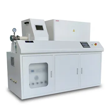
- Chemical Vapor Deposition CVD Equipment System Chamber Slide PECVD Tube Furnace with Liquid Gasifier PECVD Machine
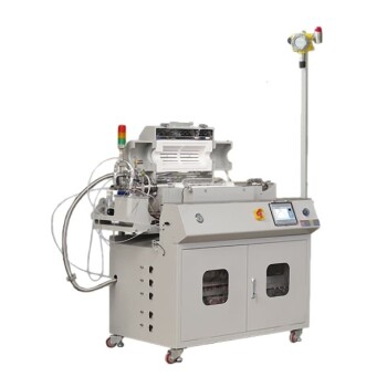
- Customer Made Versatile CVD Tube Furnace Chemical Vapor Deposition Chamber System Equipment
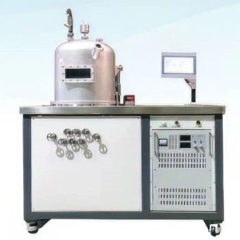
- HFCVD Machine System Equipment for Drawing Die Nano-Diamond Coating
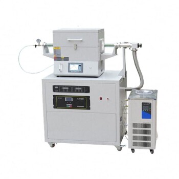
- Split Chamber CVD Tube Furnace with Vacuum Station Chemical Vapor Deposition System Equipment Machine
- Multi Heating Zones CVD Tube Furnace Machine Chemical Vapor Deposition Chamber System Equipment
People Also Ask
- What are the advantages of chemical vapor deposition? Achieve Superior Thin Films for Your Lab
- What are the core advantages of PE-CVD in OLED encapsulation? Protect Sensitive Layers with Low-Temp Film Deposition
- How are carbon nanotubes grown? Master Scalable Production with Chemical Vapor Deposition
- What are the processes of vapor phase deposition? Understand CVD vs. PVD for Superior Thin Films
- What happens during deposition chemistry? Building Thin Films from Gaseous Precursors
