In essence, the Chemical Vapor Deposition (CVD) process is a highly controlled, five-stage sequence. It begins with the transport of reactive precursor gases into a chamber, followed by their diffusion to a heated substrate. The gases then adsorb onto the substrate's surface, undergo a chemical reaction to form a solid film, and finally, the gaseous byproducts of this reaction are removed from the chamber.
Chemical Vapor Deposition is not a simple coating method; it is a sophisticated materials synthesis technique governed by a precise sequence of gas transport phenomena and surface-level chemical reactions. Understanding the journey of a molecule from the gas inlet to its final place in the film is key to mastering the process.

Deconstructing the CVD Process: A Step-by-Step Analysis
To truly grasp CVD, we must break it down into its fundamental physical and chemical stages. Each step presents a potential bottleneck that can influence the quality and growth rate of the final film.
Step 1: Introducing the Precursor Gases
The process begins by introducing a carefully managed mixture of reactive gases, known as precursors, into the reaction chamber.
These precursors are volatile compounds containing the elements you wish to deposit. They are transported via convection and diffusion from their source into the main volume of the reactor.
Step 2: Navigating the Boundary Layer
As the gases flow over the heated substrate, a thin, stagnant layer of gas called the boundary layer forms just above the surface.
Reactant molecules must diffuse across this layer to reach the substrate. This step is often the rate-limiting factor in the entire CVD process, as it controls the supply of reactants to the surface.
Step 3: Adsorption onto the Surface
Once a reactant molecule successfully crosses the boundary layer, it must physically stick to the substrate's surface. This process is called adsorption.
This initial attachment can be a weak physical bond (physisorption) or a stronger chemical bond (chemisorption), preparing the molecule for the subsequent reaction.
Step 4: The Surface Reaction and Film Growth
With reactants adsorbed onto the heated surface, they gain enough thermal energy to react. This is a heterogeneous surface reaction, meaning it occurs at the interface between the gas/solid phases.
These reactions break down the precursor molecules, depositing the desired solid material and creating volatile byproducts. The deposited atoms then diffuse across the surface to find stable nucleation sites, forming the initial islands of the film that eventually grow and coalesce into a continuous layer.
Step 5: Removing the Byproducts
The volatile byproducts created during the surface reaction must be removed. They desorb (detach) from the surface, diffuse back out through the boundary layer, and are then swept away by the main gas flow out of the reactor.
Efficient removal of byproducts is critical to prevent their incorporation as impurities in the growing film and to avoid interfering with the ongoing deposition reaction.
Critical Parameters That Control the Process
The outcome of these five steps is not left to chance. It is dictated by several key process parameters that engineers and scientists manipulate to achieve the desired film properties.
Temperature: The Engine of Reaction
Substrate temperature is arguably the most crucial parameter. It provides the energy needed to drive the surface reactions and can influence everything from growth rate to the film's crystalline structure. Typical temperatures can range up to 1000–1100 °C.
Pressure: Dictating Molecular Interactions
The pressure inside the reactor chamber determines the concentration of gas molecules and the thickness of the boundary layer. Lower pressures can improve film uniformity but may reduce the deposition rate.
Gas Flow and Composition: The Supply Chain
The flow rate and ratio of precursor gases act as the process's supply chain. They control the availability of reactants, directly impacting the growth rate and stoichiometry (elemental composition) of the final film.
Understanding the Trade-offs and Pitfalls
CVD is a powerful technique, but it comes with inherent challenges. Acknowledging these trade-offs is essential for successful implementation.
Uniformity vs. Growth Rate
Achieving a perfectly uniform film thickness across a large substrate can be difficult. Often, process conditions that favor high growth rates (e.g., high pressure) can lead to depletion of reactants downstream, causing the film to be thinner at the edges.
Purity and Contamination
The final film is highly sensitive to impurities. Any residual moisture or oxygen in the chamber can react with the substrate or precursors, leading to contamination. This is why a thorough purging of the chamber before deposition is essential.
Substrate Compatibility
The CVD process must be compatible with the substrate material. The high temperatures involved can damage sensitive substrates, and the surface chemistry must be suitable for the adsorption and nucleation of the desired film.
Making the Right Choice for Your Goal
Your primary objective will determine which aspects of the CVD process you should focus on for control and optimization.
- If your primary focus is high-speed production: You must optimize the mass transport of reactants through the boundary layer by adjusting pressure and flow rates.
- If your primary focus is ultimate film purity: Prioritize high-purity precursor gases and the efficient desorption and removal of reaction byproducts.
- If your primary focus is process consistency: Pay closest attention to precise control over substrate temperature and the stability of your gas flow system.
Ultimately, mastering CVD is about managing the journey of molecules from gas to a functional solid film.
Summary Table:
| CVD Process Step | Key Action | Purpose |
|---|---|---|
| 1. Gas Transport | Introduce precursor gases into the chamber | Deliver reactants to the substrate |
| 2. Diffusion | Molecules cross the boundary layer | Reach the heated substrate surface |
| 3. Adsorption | Molecules stick to the substrate surface | Prepare for chemical reaction |
| 4. Surface Reaction | Chemical reaction forms the solid film | Deposit the desired material |
| 5. Byproduct Removal | Remove volatile byproducts from the chamber | Ensure film purity and process efficiency |
Ready to optimize your Chemical Vapor Deposition process?
At KINTEK, we specialize in providing high-performance lab equipment and consumables tailored for advanced materials synthesis. Whether you are focused on achieving ultimate film purity, high-speed production, or process consistency, our expertise and solutions can help you master the CVD journey from gas to film.
Contact us today to discuss how our specialized equipment can enhance your laboratory's capabilities and drive your research forward.
Visual Guide

Related Products
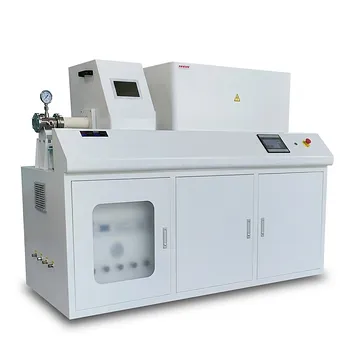
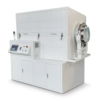
- Chemical Vapor Deposition CVD Equipment System Chamber Slide PECVD Tube Furnace with Liquid Gasifier PECVD Machine
- Inclined Rotary Plasma Enhanced Chemical Vapor Deposition PECVD Equipment Tube Furnace Machine
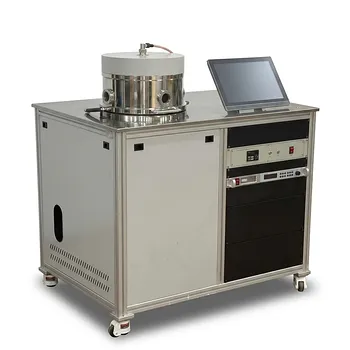
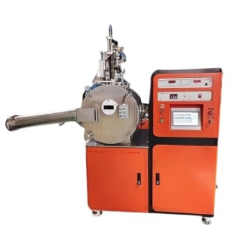
- RF PECVD System Radio Frequency Plasma-Enhanced Chemical Vapor Deposition RF PECVD
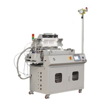
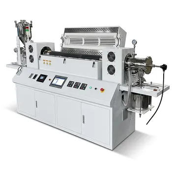
- Customer Made Versatile CVD Tube Furnace Chemical Vapor Deposition Chamber System Equipment
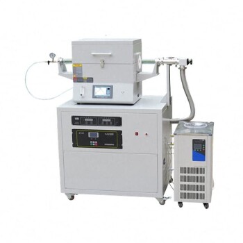
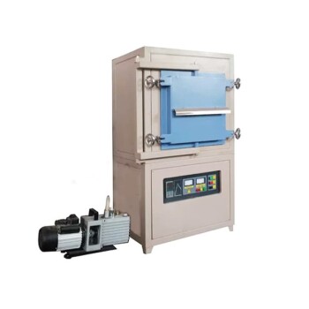
- Split Chamber CVD Tube Furnace with Vacuum Station Chemical Vapor Deposition System Equipment Machine
People Also Ask
- What color diamonds are CVD? Understanding the Process from Brown Tint to Colorless Beauty
- What are the methods of deposition? A Guide to PVD and CVD Thin-Film Techniques
- What is PECVD in semiconductor? Enable Low-Temperature Thin Film Deposition for ICs
- How does PECVD work? Enable Low-Temperature, High-Quality Thin Film Deposition
- What are the different types of thin films? A Guide to Optical, Electrical, and Functional Coatings
