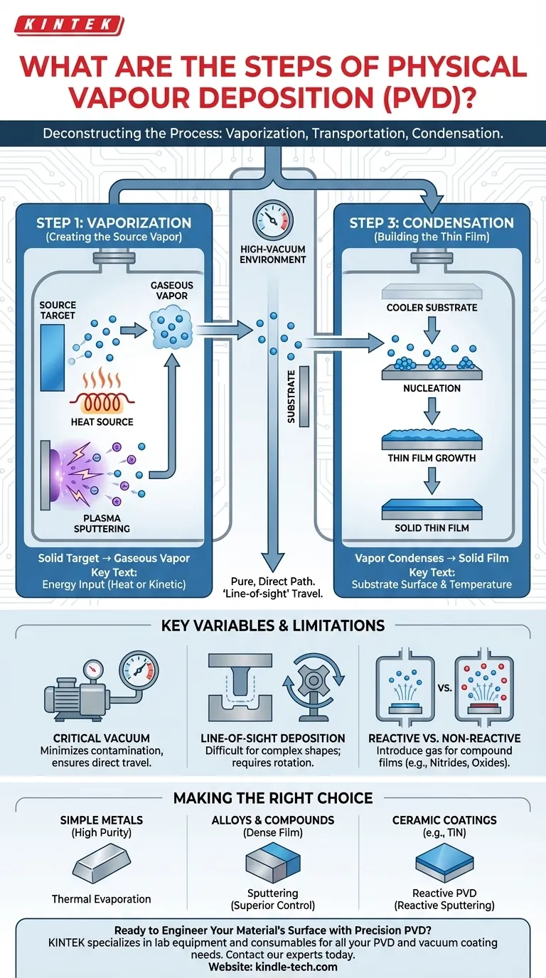
In principle, all Physical Vapor Deposition (PVD) processes are built on three fundamental steps: vaporization of a source material, transportation of that vapor across a vacuum, and its condensation onto a substrate to form a solid film. These core actions are the foundation of any PVD technique, from simple thermal evaporation to complex plasma sputtering.
Physical Vapor Deposition is not a single process, but a category of vacuum deposition methods. Despite their differences, all PVD techniques share the same universal principle: converting a solid material into a vapor, transporting it, and condensing it to create a high-performance thin film.
Deconstructing the PVD Process
Every PVD coating, regardless of the specific equipment used, is the result of a carefully controlled three-step physical sequence. The primary difference between various PVD methods lies in how the first step, vaporization, is accomplished.
Step 1: Vaporization (Creating the Source Vapor)
This initial step involves transforming a solid or liquid source material, known as the "target," into a gaseous vapor. This is achieved by supplying energy to the target material inside a vacuum chamber.
The two most common methods for this are:
- Thermal Evaporation: The source material is heated using methods like resistance heating or electron beams. As the temperature rises, the material's atoms gain enough energy to evaporate, turning directly into a gas.
- Sputtering: Instead of heat, this method uses kinetic energy. A high-energy plasma is created, and ions from this plasma are accelerated to strike the target material. This high-energy bombardment physically knocks atoms loose from the target's surface, ejecting them into the chamber.
Step 2: Transportation (Moving the Vapor to the Substrate)
Once vaporized, the atoms or molecules travel from the source target toward the object to be coated, called the substrate.
This transport phase occurs in a high-vacuum environment. The vacuum is critical because it removes air and other gas molecules that could collide with and contaminate the vaporized material, ensuring a pure and direct path to the substrate. This is often referred to as "line-of-sight" travel.
Step 3: Condensation (Building the Thin Film)
When the vaporized atoms reach the cooler surface of the substrate, they lose their energy and condense back into a solid state.
This condensation does not happen all at once. It begins with nucleation, where individual atoms stick to the surface and form small islands. These islands then grow and merge, eventually forming a continuous, dense, and tightly bonded thin film across the entire substrate.
Understanding Key Variables and Limitations
The success of a PVD process depends on precise control over its environment. Understanding the trade-offs and common challenges is essential for achieving the desired coating properties.
The Critical Role of Vacuum
A high vacuum is non-negotiable in PVD. It serves two primary functions: it minimizes the chance of the vaporized atoms reacting with unwanted gases like oxygen or nitrogen, and it increases the "mean free path," allowing atoms to travel directly to the substrate without collisions. An insufficient vacuum leads to contaminated, porous, and poorly adhered films.
The Challenge of Line-of-Sight Deposition
Because vapor particles travel in a straight line, basic PVD has difficulty coating complex, three-dimensional shapes with undercuts or hidden surfaces. The coating will only form on areas with a direct line of sight to the source material. More advanced setups use rotating fixtures to expose all surfaces of the substrate to the vapor stream.
Reactive vs. Non-Reactive Processes
In its simplest form, PVD deposits a film of the exact same material as the target (e.g., titanium vapor deposits a titanium film). However, by intentionally introducing a small, controlled amount of a "reactive gas" (like nitrogen or oxygen) into the chamber, you can form compound films. For example, a titanium target sputtered in a nitrogen atmosphere will create a hard, gold-colored titanium nitride (TiN) coating.
Making the Right Choice for Your Goal
The specific PVD method you choose depends entirely on the material you are depositing and the properties you need in the final film.
- If your primary focus is coating simple, pure metals with high purity: Thermal evaporation is often the simplest and most cost-effective method.
- If your primary focus is depositing alloys, compounds, or achieving a very dense film: Sputtering offers superior control over composition and results in better film adhesion and density.
- If your primary focus is creating a ceramic coating like a nitride or oxide: Reactive PVD (usually reactive sputtering) is the required approach to form the compound during deposition.
Ultimately, PVD is a versatile family of techniques that provides a powerful toolbox for precisely engineering the surfaces of materials.
Summary Table:
| Step | Key Action | Critical Factor |
|---|---|---|
| 1. Vaporization | Solid target material is converted into a vapor. | Energy input (heat for evaporation, kinetic for sputtering). |
| 2. Transportation | Vapor travels to the substrate. | High-vacuum environment for a pure, direct path. |
| 3. Condensation | Vapor condenses to form a solid thin film. | Substrate temperature and surface condition for adhesion. |
Ready to Engineer Your Material's Surface with Precision PVD?
The right PVD method is critical for achieving the perfect thin film—whether you need high-purity metal coatings, dense alloy films, or hard ceramic compounds like titanium nitride. KINTEK specializes in lab equipment and consumables for all your PVD and vacuum coating needs, helping you select the ideal setup for your specific material and performance goals.
Contact our experts today to discuss how we can support your laboratory's thin film deposition projects and enhance your research capabilities.
Visual Guide
Related Products
- HFCVD Machine System Equipment for Drawing Die Nano-Diamond Coating
- Custom CVD Diamond Coating for Lab Applications
- Electron Beam Evaporation Coating Oxygen-Free Copper Crucible and Evaporation Boat
- Chemical Vapor Deposition CVD Equipment System Chamber Slide PECVD Tube Furnace with Liquid Gasifier PECVD Machine
- Infrared Transmission Coating Sapphire Sheet Substrate Window
People Also Ask
- What are the disadvantages and challenges of the HFCVD method? Overcome Growth Limits and Filament Issues
- Why is Chemical Vapor Deposition (CVD) equipment uniquely suited for constructing hierarchical superhydrophobic structures?
- What is the function of tungsten filaments in HFCVD? Powering Diamond Film Synthesis with Thermal Excitation
- What is the full form of HFCVD? A Guide to Hot Filament Chemical Vapor Deposition
- What is the chemical vapor deposition growth process? Build Superior Thin Films from the Atom Up


