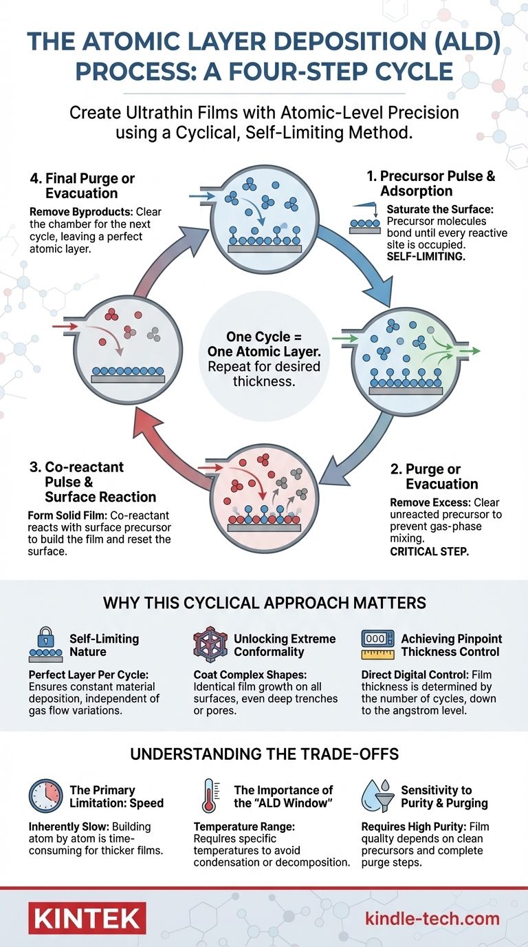
At its core, Atomic Layer Deposition (ALD) is a cyclical process for creating ultrathin films with atomic-level precision. A complete ALD cycle consists of four distinct, sequential steps: a precursor pulse, a purge of excess precursor, a co-reactant pulse, and a final purge of excess co-reactant and byproducts. This deliberate separation of reactants is the key to its unique capabilities.
The defining characteristic of ALD is its self-limiting nature. By separating the chemical reactions into two distinct half-reactions, the process ensures that only one atomic layer of material can be deposited per cycle, granting unparalleled control over film thickness and uniformity.
The ALD Cycle in Detail
To understand why ALD is so powerful, we must examine the purpose of each step in its fundamental four-part cycle. Imagine you are painting a wall one single layer of molecules at a time.
Step 1: Precursor Pulse and Adsorption
The first chemical, known as the precursor, is pulsed into the reaction chamber as a gas. These molecules spread throughout the chamber and chemically bond (chemisorb) to the surface of the object you want to coat (the substrate).
This reaction is self-limiting. Once every available reactive site on the surface is occupied by a precursor molecule, no more can attach. The surface is now saturated.
Step 2: Purge or Evacuation
Next, the chamber is cleared of all the excess, unreacted precursor molecules. This is typically done by pumping them out (evacuation) or by flushing the chamber with an inert gas like nitrogen or argon.
This step is critical. It ensures that the first and second chemicals will never mix in the gas phase, which would cause uncontrolled deposition and defeat the purpose of ALD.
Step 3: Co-reactant Pulse and Surface Reaction
The second chemical, the co-reactant (often something simple like water vapor or ozone), is then pulsed into the chamber.
This co-reactant does not react with the surface itself. Instead, it reacts exclusively with the precursor molecules that are already chemically bonded to the surface from Step 1. This reaction forms the desired solid material (e.g., Al₂O₃) and prepares the new surface to react with the precursor again.
Step 4: Final Purge or Evacuation
Finally, the chamber is purged a second time to remove any unreacted co-reactant molecules and any gaseous byproducts created during the reaction in Step 3.
At the end of this step, you are left with a single, pristine, and complete atomic layer of your target material. The surface is now reset and ready for the next cycle to begin, starting again with Step 1.
Why This Cyclical Approach Matters
The separation of reactions is not just a procedural detail; it is the very source of ALD's primary advantages over other thin-film deposition techniques.
The Self-Limiting Nature
Because each half-reaction (Steps 1 and 3) only proceeds until the surface is saturated, the amount of material deposited in one cycle is constant. It does not depend on having a perfectly uniform flow of gas. This inherent self-control is what guarantees a perfect layer is added with every single cycle.
Unlocking Extreme Conformality
This surface-controlled growth allows ALD to coat incredibly complex, 3D structures with perfect uniformity. Since the precursor gas can reach any exposed surface—no matter how deep inside a trench or pore—the film grows identically everywhere. This is known as high conformality and is extremely difficult to achieve with line-of-sight methods like sputtering.
Achieving Pinpoint Thickness Control
The final thickness of an ALD film is determined simply by the number of cycles performed. If one cycle deposits 0.1 nanometers of material, then 100 cycles will deposit exactly 10 nanometers. This gives engineers direct, digital control over film thickness at the angstrom level.
Understanding the Trade-offs
No technology is without its limitations, and ALD's precision comes at a cost.
The Primary Limitation: Speed
Building a film one atomic layer at a time is inherently slow. Each of the four steps takes time, meaning a single cycle can last from a fraction of a second to several seconds. Growing a film that is hundreds of nanometers thick can be prohibitively time-consuming and expensive for many applications.
The Importance of the "ALD Window"
The self-limiting behavior only occurs within a specific range of temperatures. If the temperature is too low, the chemicals can condense on the surface like water on a cold glass. If it's too high, the precursor may decompose on its own or fail to stick to the surface, leading to uncontrolled, CVD-like growth and poor film quality.
Sensitivity to Purity and Purging
The quality of the final film is highly dependent on the purity of the precursor chemicals and the completeness of the purge steps. If a purge step is incomplete, residual chemicals can cause unwanted reactions, introducing impurities into the film and degrading its performance.
Is ALD the Right Process for Your Application?
Choosing a deposition method requires balancing precision with practicality. Your end goal will determine if ALD is the right tool for the job.
- If your primary focus is ultimate precision and conformality: ALD is the superior choice for coating complex 3D nanostructures, such as those in modern microchips, or when angstrom-level thickness control is non-negotiable.
- If your primary focus is speed and cost for thicker films: Traditional methods like Chemical Vapor Deposition (CVD) or Physical Vapor Deposition (PVD) are often more practical and economical for applications that do not require atomic-level control.
By understanding its unique, self-limiting cyclical nature, you can leverage ALD's precision for the most demanding thin-film applications.
Summary Table:
| Step | Purpose | Key Action |
|---|---|---|
| 1. Precursor Pulse | Saturate the surface | First chemical (precursor) bonds to the substrate |
| 2. Purge | Remove excess precursor | Inert gas flush or evacuation |
| 3. Co-reactant Pulse | Form the solid film | Second chemical reacts with surface-bound precursor |
| 4. Final Purge | Remove byproducts and excess co-reactant | Chamber is cleared for the next cycle |
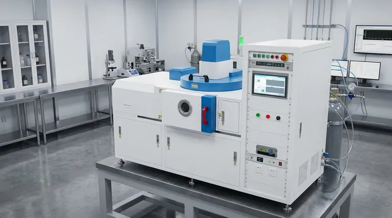
Need to deposit ultra-precise, conformal thin films for your research or production? KINTEK specializes in providing high-quality lab equipment and consumables, including ALD systems, to help you achieve atomic-level control over your coatings. Whether you're working on semiconductor devices, nanotechnology, or advanced materials, our solutions are designed to meet the demanding requirements of modern laboratories. Contact us today to discuss how our ALD expertise can enhance your project's precision and performance!
Visual Guide
Related Products
- Chemical Vapor Deposition CVD Equipment System Chamber Slide PECVD Tube Furnace with Liquid Gasifier PECVD Machine
- RF PECVD System Radio Frequency Plasma-Enhanced Chemical Vapor Deposition RF PECVD
- HFCVD Machine System Equipment for Drawing Die Nano-Diamond Coating
- 915MHz MPCVD Diamond Machine Microwave Plasma Chemical Vapor Deposition System Reactor
- Inclined Rotary Plasma Enhanced Chemical Vapor Deposition PECVD Equipment Tube Furnace Machine
People Also Ask
- What is the chemical vapor deposition growth process? Build Superior Thin Films from the Atom Up
- How are carbon nanotubes grown? Master Scalable Production with Chemical Vapor Deposition
- What are the processes of vapor phase deposition? Understand CVD vs. PVD for Superior Thin Films
- How expensive is chemical vapor deposition? Understanding the True Cost of High-Performance Coating
- What types of substrates are used in CVD to facilitate graphene films? Optimize Graphene Growth with the Right Catalyst


