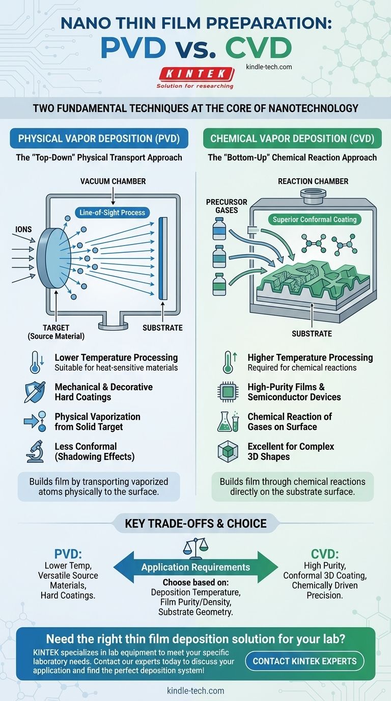
At the core of nanotechnology, the two fundamental techniques for preparing nano thin films are Physical Vapor Deposition (PVD) and Chemical Vapor Deposition (CVD). These processes represent two distinct philosophies for building a film atom by atom: one physically transports material to a surface, while the other uses chemical reactions to grow the film directly on it.
The essential difference lies in the state of the source material. PVD is a "line-of-sight" physical process that vaporizes a solid target, while CVD is a chemical process that uses precursor gases to react and form a solid film on a substrate.
Understanding Physical Vapor Deposition (PVD)
Physical Vapor Deposition encompasses a set of vacuum deposition methods where a material is transformed into its vapor phase, transported through a vacuum, and then condensed onto a substrate as a solid thin film. It is fundamentally a physical transport phenomenon.
The "Top-Down" Principle
PVD is often considered a "top-down" approach. A solid or liquid source material, known as the "target," is vaporized through physical means like heating or ion bombardment.
These vaporized atoms or molecules then travel through a vacuum or low-pressure environment and deposit onto the surface of the object being coated, known as the "substrate."
How PVD Works
The entire process occurs inside a vacuum chamber to prevent the vaporized material from reacting with particles in the air. Common PVD methods include sputtering, where high-energy ions bombard the target, and thermal evaporation, where the target is heated until it vaporizes.
Because the atoms travel in a straight line from the target to the substrate, PVD is often called a line-of-sight process.
Understanding Chemical Vapor Deposition (CVD)
Chemical Vapor Deposition is a process where a substrate is exposed to one or more volatile chemical precursors. These precursors react or decompose on the substrate's surface to produce the desired thin film deposit.
The "Bottom-Up" Principle
CVD is a "bottom-up" method where the film is built through chemical reactions. The process does not physically transfer an existing material but rather creates a new solid material directly on the substrate.
The properties of the final film are determined by the chemistry of the precursor gases, the temperature of the reaction, and the pressure within the chamber.
Superior Conformal Coating
Because the precursor gases can flow around and into complex geometries, CVD is exceptionally good at producing conformal coatings. This means it can deposit a film of uniform thickness over intricate and non-flat surfaces, which is a significant advantage over line-of-sight PVD methods.
Key Trade-offs: PVD vs. CVD
Choosing the right deposition technique is critical because, as the references note, the method determines virtually all the properties of the final film. The decision involves balancing requirements for temperature, film quality, and geometry.
Deposition Temperature
PVD processes can often be conducted at lower temperatures than many CVD processes. This makes PVD suitable for coating materials that are sensitive to heat, such as certain plastics or polymers.
CVD typically requires high temperatures to drive the necessary chemical reactions, which can limit the types of substrates that can be used.
Film Purity and Density
CVD can often produce films of higher purity and with fewer defects than PVD. The chemical nature of the process allows for greater control over stoichiometry and can result in denser, more robust films.
Substrate Geometry
CVD's ability to coat complex, three-dimensional shapes uniformly is its primary advantage. PVD struggles with "shadowing" effects on non-flat surfaces due to its line-of-sight nature.
Making the Right Choice for Your Application
Your choice between these two foundational techniques depends entirely on the specific requirements of your end product and the material you are working with.
- If your primary focus is coating complex 3D shapes or achieving maximum film purity: CVD is often the superior choice due to its excellent conformality and chemically driven precision.
- If your primary focus is coating heat-sensitive substrates or depositing metal alloys: PVD's lower processing temperatures and versatility with source materials provide a distinct advantage.
- If your primary focus is on mechanical or decorative hard coatings: PVD techniques like sputtering are industry standards for creating durable, wear-resistant surfaces on tools and components.
Ultimately, both PVD and CVD are powerful platforms for engineering materials at the nanoscale, each offering a unique set of capabilities to solve specific challenges.
Summary Table:
| Technique | Core Principle | Key Advantage | Typical Use Case |
|---|---|---|---|
| Physical Vapor Deposition (PVD) | Physical transport of vaporized material | Lower temperature processing | Coating heat-sensitive substrates, metal alloys, decorative/hard coatings |
| Chemical Vapor Deposition (CVD) | Chemical reaction of precursor gases | Superior conformal coating on complex 3D shapes | High-purity films, semiconductor devices, intricate components |
Need the right thin film deposition solution for your lab? Choosing between PVD and CVD is critical for your project's success. KINTEK specializes in lab equipment and consumables, providing the expertise and technology to meet your specific laboratory needs. Contact our experts today to discuss your application and find the perfect deposition system!
Visual Guide
Related Products
- Vacuum Hot Press Furnace Machine for Lamination and Heating
- HFCVD Machine System Equipment for Drawing Die Nano-Diamond Coating
- Electron Beam Evaporation Coating Oxygen-Free Copper Crucible and Evaporation Boat
- Molybdenum Tungsten Tantalum Evaporation Boat for High Temperature Applications
- Laboratory Micro Horizontal Jar Mill for Precision Sample Preparation in Research and Analysis
People Also Ask
- What role does the high vacuum environment play in sintering graphite film/aluminum composites? Optimize Your Bonding
- What is the purpose of remelting heat treatment in a vacuum hot press for UHMWPE? Ensure Oxidative Stability
- What advantages does a vacuum hot press furnace provide for LSLBO ceramic electrolytes? Achieve 94% Relative Density
- How does a vacuum hot press furnace contribute to the molding process of UHMWPE/nano-HAP composites?
- What are the advantages of using a vacuum hot press furnace for sintering CNT/Cu composites? Superior Density & Bonding