In essence, chemical vapor deposition (CVD) is a foundational manufacturing process used to create high-performance thin films and coatings on a variety of materials. Its primary uses are in the electronics industry for fabricating semiconductor devices, in manufacturing for applying durable protective coatings to cutting tools and automotive parts, and in the energy sector for producing thin-film solar cells.
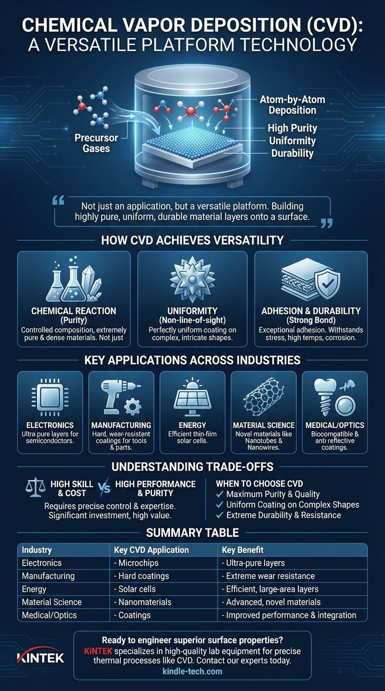
Chemical vapor deposition should not be viewed as a single application, but as a versatile platform technology. Its true value lies in its ability to build highly pure, uniform, and durable material layers onto a surface, atom by atom, enabling the creation of components with precisely engineered surface properties.
How CVD Achieves This Versatility
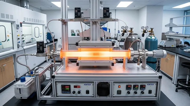
Chemical vapor deposition is a process where a substrate (the object to be coated) is placed in a vacuum chamber and exposed to one or more volatile precursor gases. The chamber is heated, causing a chemical reaction or decomposition of these gases on and near the substrate's surface, resulting in the deposition of a thin, solid film.
The Power of Chemical Reaction
Unlike physical deposition methods that essentially spray a material, CVD builds a film through a chemical transformation at the surface. This allows for the creation of extremely pure and dense materials.
The composition of the final film is controlled by the precursor gases used, making the process highly versatile for creating metallic, ceramic, or semiconducting layers.
Uniformity on Complex Shapes
Because the deposition occurs from a gas phase that envelops the entire substrate, CVD is a non-line-of-sight process.
This is a critical advantage, as it allows for a perfectly uniform coating to be applied over complex, intricate, and three-dimensional surfaces, which is difficult or impossible with line-of-sight methods.
Superior Adhesion and Durability
The chemical bonding that occurs between the deposited film and the substrate results in exceptional adhesion. The resulting coatings are dense and robust, able to withstand significant mechanical stress, high temperatures, and corrosive environments.
Key Applications Across Industries
The unique capabilities of CVD make it indispensable in sectors where surface performance is critical.
The Foundation of Modern Electronics
The semiconductor industry relies heavily on CVD to deposit the ultra-pure, exceptionally thin layers of conducting, semiconducting, and insulating materials that form microchips. The process's precision is essential for creating today's complex integrated circuits.
Enhancing Industrial Durability
CVD is used to apply hard, wear-resistant coatings (like titanium nitride) onto cutting tools, drills, and machine parts. This dramatically increases their lifespan, reduces friction, and protects against corrosion. Similar coatings are used on automotive engine parts for improved durability.
Powering Renewable Energy
In the manufacturing of thin-film solar cells, CVD is used to deposit layers of photovoltaic materials onto a substrate, such as glass. The process's ability to create uniform, large-area films is key to producing efficient and cost-effective solar panels.
Advancing Material Science
Researchers use CVD to grow novel materials with unique properties, such as carbon nanotubes and gallium nitride (GaN) nanowires. These advanced materials are foundational to next-generation electronics, composites, and sensors.
Protecting Medical and Optical Devices
Biocompatible coatings can be applied to medical implants to improve their integration with the body and reduce rejection. In optics, CVD is used to create anti-reflective coatings or layers for specialized components like holographic displays.
Understanding the Trade-offs
While powerful, CVD is not a universal solution. Its effective implementation requires understanding its specific demands and limitations.
Requires High-Skill Operation
Achieving a high-quality, repeatable deposition requires precise control over numerous variables, including temperature, pressure, gas flow rates, and chamber chemistry. This demands significant operator skill and process expertise.
Material and Temperature Constraints
The substrate material must be able to withstand the high temperatures often required for the chemical reaction to occur, which can range from 200°C to over 1600°C. Furthermore, the precursor chemicals must be volatile enough to exist as a gas but stable enough not to decompose prematurely.
Cost vs. Performance
While described as relatively affordable for the performance it delivers, the initial investment in vacuum chambers and high-purity gas handling systems can be substantial. It is a high-value process chosen when the performance and purity of the coating justify the operational complexity.
When to Choose Chemical Vapor Deposition
Your decision to use CVD should be based on the specific performance requirements of your component.
- If your primary focus is maximum material purity and crystalline quality: CVD is the industry standard for applications like semiconductor manufacturing where even trace impurities can cause device failure.
- If your primary focus is a uniform coating on a complex shape: CVD's non-line-of-sight nature makes it the ideal choice for coating intricate parts that other methods cannot cover evenly.
- If your primary focus is extreme durability and environmental resistance: CVD is superior for creating hard, dense coatings that must withstand high stress, abrasion, corrosion, or extreme temperatures.
Ultimately, CVD empowers engineers to design material properties from the atoms up, building performance directly onto the surface of a component.
Summary Table:
| Industry | Key CVD Application | Key Benefit |
|---|---|---|
| Electronics | Semiconductor manufacturing | Ultra-pure, precise layers for microchips |
| Manufacturing | Hard coatings for tools & parts | Extreme wear resistance & durability |
| Energy | Thin-film solar cells | Efficient, large-area photovoltaic layers |
| Material Science | Growth of nanotubes & nanowires | Creation of advanced, novel materials |
| Medical/Optics | Biocompatible & anti-reflective coatings | Improved device performance & integration |
Ready to engineer superior surface properties for your components?
Chemical Vapor Deposition is a powerful platform for creating high-purity, uniform, and durable coatings that are essential for advanced manufacturing and R&D. Whether you are developing next-generation semiconductors, need wear-resistant coatings for industrial tools, or are researching novel materials, the right equipment is critical.
KINTEK specializes in providing high-quality lab equipment and consumables for precise thermal processes like CVD. Our solutions help laboratories and manufacturers achieve repeatable, high-performance results.
Contact our experts today to discuss how we can support your specific application needs and help you leverage the power of CVD technology.
Visual Guide
Related Products
- Chemical Vapor Deposition CVD Equipment System Chamber Slide PECVD Tube Furnace with Liquid Gasifier PECVD Machine
- RF PECVD System Radio Frequency Plasma-Enhanced Chemical Vapor Deposition RF PECVD
- Microwave Plasma Chemical Vapor Deposition MPCVD Machine System Reactor for Lab and Diamond Growth
- Customer Made Versatile CVD Tube Furnace Chemical Vapor Deposition Chamber System Equipment
- 915MHz MPCVD Diamond Machine Microwave Plasma Chemical Vapor Deposition System Reactor
People Also Ask
- What types of substrates are used in CVD to facilitate graphene films? Optimize Graphene Growth with the Right Catalyst
- Why is Chemical Vapor Deposition (CVD) equipment uniquely suited for constructing hierarchical superhydrophobic structures?
- What are the advantages of chemical vapor deposition? Achieve Superior Thin Films for Your Lab
- How are carbon nanotubes grown? Master Scalable Production with Chemical Vapor Deposition
- What is the chemical vapor deposition growth process? Build Superior Thin Films from the Atom Up


