In short, PECVD is a foundational thin-film deposition technology used across a vast range of high-tech industries. Its primary applications are in manufacturing semiconductor devices, creating advanced optical coatings, and applying durable, functional surfaces for mechanical parts, medical implants, and even food packaging.
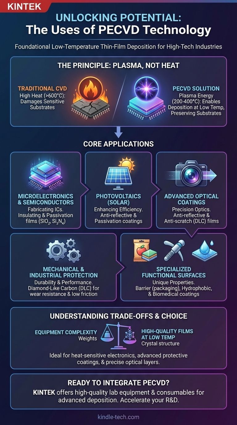
The core value of Plasma-Enhanced Chemical Vapor Deposition (PECVD) is its ability to deposit high-quality, dense films at much lower temperatures than conventional methods. This single advantage makes it indispensable for creating sophisticated materials on substrates that cannot withstand high heat.
The Principle: Why Low Temperature Is a Game-Changer
PECVD, or Plasma-Enhanced Chemical Vapor Deposition, solves a fundamental manufacturing problem: how to grow a high-quality material layer without melting or damaging what's underneath.
The Problem with Heat
Traditional Chemical Vapor Deposition (CVD) relies on high temperatures (often >600°C) to provide the energy needed for chemical reactions to occur and form a film on a substrate.
This works for robust materials but is destructive for complex devices like integrated circuits or heat-sensitive substrates like plastics.
The PECVD Solution: Plasma, Not Heat
PECVD circumvents the need for extreme heat by using an electric field to generate a plasma—an energized state of gas.
This plasma provides the energy to break apart precursor gas molecules and drive the chemical reactions, allowing a high-quality film to deposit at significantly lower temperatures (typically 200-400°C).
Core Applications of PECVD
This low-temperature capability has made PECVD a critical process in numerous fields where material performance and substrate integrity are paramount.
Microelectronics and Semiconductors
This is the most widespread use of PECVD. It is essential for fabricating the billions of transistors found in a modern integrated circuit (IC).
Its key roles include depositing dielectric (insulating) films like silicon dioxide (SiO₂) and silicon nitride (Si₃N₄). These films isolate conductive layers, form capacitors, and provide surface passivation—a final protective layer that shields the delicate chip from moisture and contamination.
Photovoltaics (Solar Cells)
PECVD is used extensively in manufacturing solar cells. It deposits critical layers, such as anti-reflective coatings that maximize light absorption and passivation layers that improve the cell's overall efficiency and lifespan.
Advanced Optical Coatings
The ability to deposit precise, uniform layers makes PECVD ideal for optics. It is used to create anti-reflective coatings on lenses and displays to reduce glare and improve light transmission.
It is also used for applying hard, anti-scratch coatings to eyeglasses, camera lenses, and other optical components.
Mechanical and Industrial Protection
PECVD can apply exceptionally hard and slick coatings to improve the durability and performance of mechanical parts.
A primary example is Diamond-Like Carbon (DLC) coatings, which provide extreme wear resistance and low friction for tools, automotive components, and industrial machinery. It is also used to coat pipelines to protect against corrosion.
Specialized Functional Surfaces
The versatility of PECVD extends to creating surfaces with unique properties. This includes:
- Barrier Coatings: For food packaging and bottling, PECVD creates a transparent, flexible barrier film that blocks moisture and oxygen, extending shelf life.
- Hydrophobic Coatings: These water-repelling films are used in diverse applications, from self-cleaning surfaces to microfluidic devices.
- Biomedical Coatings: PECVD is used to coat medical implants to improve biocompatibility, reduce friction, and prevent rejection by the body.
Understanding the Trade-offs
While incredibly versatile, PECVD is not a universal solution. The choice to use it involves clear trade-offs against other deposition methods.
Equipment Complexity and Cost
PECVD systems require a vacuum chamber, gas handling, and high-frequency power supplies to generate the plasma. This makes the equipment more complex and costly than simpler methods like atmospheric pressure CVD or thermal oxidation.
Film Properties vs. Temperature
The primary trade-off is between processing temperature and film quality. While PECVD films are high quality for their low deposition temperature, films deposited with higher-temperature processes like LPCVD (Low-Pressure CVD) can sometimes exhibit superior properties, such as better uniformity or lower impurities.
However, if the substrate is an integrated circuit with aluminum wiring (which melts around 660°C), the superior properties of a high-temperature film are irrelevant because the process would destroy the device. PECVD is the only viable option.
Making the Right Choice for Your Application
Selecting the right deposition technique requires aligning the process capabilities with your primary goal.
- If your primary focus is fabricating complex electronics: PECVD is non-negotiable for depositing critical insulating films without damaging previously built, heat-sensitive circuit components.
- If your primary focus is creating durable protective surfaces: PECVD offers advanced, high-performance coatings like DLC that provide superior wear, corrosion, and friction resistance.
- If your primary focus is enhancing optical components: Use PECVD for precise, uniform anti-reflective and scratch-resistant layers, especially on polymer-based or coated optics.
- If your primary focus is creating functional barriers on flexible substrates: PECVD is a leading method for applying thin, effective barrier layers for modern packaging and printable electronics.
Ultimately, PECVD empowers engineers to build better products by decoupling material deposition from the constraints of high temperature.
Summary Table:
| Application Area | Key PECVD Uses | Common Materials Deposited |
|---|---|---|
| Semiconductors | Insulating layers, surface passivation | Silicon Dioxide (SiO₂), Silicon Nitride (Si₃N₄) |
| Photovoltaics | Anti-reflective & passivation layers | Silicon Nitride (Si₃N₄) |
| Optical Coatings | Anti-reflective, anti-scratch films | Silicon Dioxide (SiO₂), Diamond-Like Carbon (DLC) |
| Industrial Protection | Wear-resistant, low-friction coatings | Diamond-Like Carbon (DLC) |
| Functional Surfaces | Barrier films, hydrophobic coatings, biomedical coatings | Various polymers & functional films |
Ready to integrate PECVD technology into your lab's workflow?
KINTEK specializes in providing high-quality lab equipment and consumables for advanced deposition processes. Whether you are developing next-generation semiconductors, durable protective coatings, or innovative optical components, our expertise can help you achieve precise, reliable results.
Contact our experts today to discuss how our solutions can meet your specific laboratory needs and accelerate your research and development.
Visual Guide
Related Products
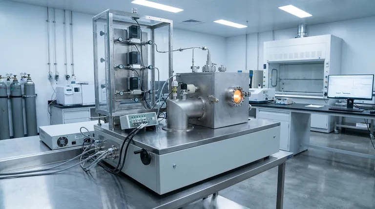
- Inclined Rotary Plasma Enhanced Chemical Vapor Deposition PECVD Equipment Tube Furnace Machine
- Chemical Vapor Deposition CVD Equipment System Chamber Slide PECVD Tube Furnace with Liquid Gasifier PECVD Machine
- Inclined Rotary Plasma Enhanced Chemical Vapor Deposition PECVD Equipment Tube Furnace Machine
- RF PECVD System Radio Frequency Plasma-Enhanced Chemical Vapor Deposition RF PECVD
- Multi Heating Zones CVD Tube Furnace Machine Chemical Vapor Deposition Chamber System Equipment
People Also Ask
- How does plasma enhanced chemical vapor deposition work? Enable Low-Temperature Thin Film Deposition
- Why is a PECVD system required for vertical graphene synthesis? Master Directional Control for 3D Nanostructures
- How does PECVD facilitate Ru-C nanocomposite films? Precision Low-Temperature Thin Film Synthesis
- How does PECVD equipment facilitate the directional growth of carbon nanotubes? Achieve Precision Vertical Alignment
- What is plasma enhanced chemical vapour deposition PECVD used for? Enable Low-Temp Thin Films for Electronics & Solar


