A primary challenge in fabricating sensing films via electroplating is the inherent variability of the deposition process itself. This variability stems from the difficulty in achieving a perfectly uniform electric field within the plating bath, which can lead to films with inconsistent thickness and, consequently, unpredictable performance.
The core issue is not simply a matter of hitting a target thickness, but ensuring that thickness is perfectly uniform across the entire active area of the sensor. This lack of uniformity is a fundamental source of inconsistent sensitivity and poor device-to-device repeatability.
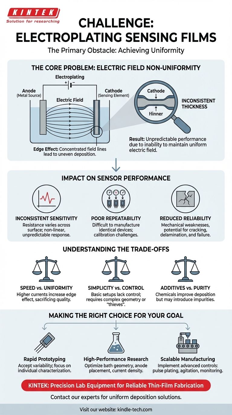
The Core Problem: Electric Field Non-Uniformity
Electroplating is a powerful technique for creating thin metal films, but its success hinges on precise control of the electrochemical environment. The distribution of the electric field is the single most critical factor.
How Electroplating Works
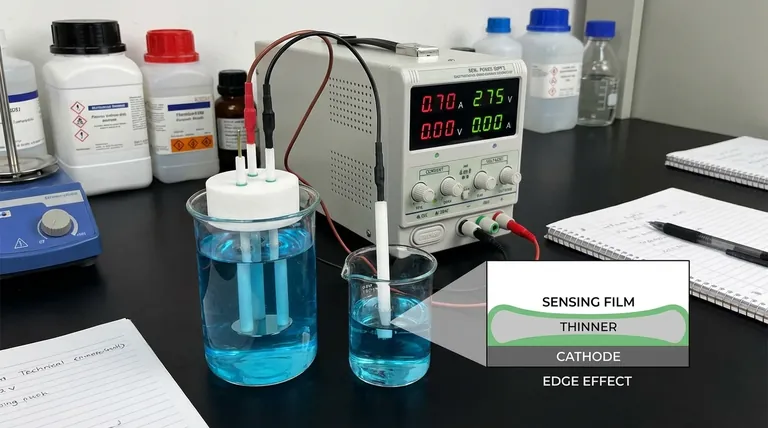
In essence, electroplating uses an electric current to reduce dissolved metal ions from a solution (the electrolyte), causing them to form a solid, thin film on the surface of a conductive object (the cathode). The rate and location of this deposition are directly controlled by the electric field.
The Source of Variation
The distribution of the electric field is rarely uniform. It is highly sensitive to the physical setup of the electroplating bath.
The geometry of the bath and the relative placement of the anode (the metal source) and the cathode (the sensing element being coated) create natural variations in current density.
The "Edge Effect"
A common manifestation of this is the "edge effect." Electric field lines tend to concentrate at sharp corners and edges of the cathode. This leads to a higher current density in these areas, causing the film to grow thicker at the edges and thinner towards the center.
The Impact on Sensing Film Performance
For a sensor, where consistency is paramount, this non-uniformity is not a minor imperfection—it is a critical flaw that directly impacts function.
Inconsistent Sensitivity
The performance of many sensors—whether they detect chemicals, pressure, or temperature—depends on the physical properties of the sensing film, such as its electrical resistance. If the film thickness varies, its resistance will also vary across its surface, leading to an unpredictable and non-linear response.
Poor Repeatability
This process variability makes it extremely difficult to manufacture multiple sensors that behave identically. If one sensor has a thicker film than another, it will have a different baseline reading and sensitivity, creating significant challenges for calibration and commercial-scale production.
Reduced Reliability
Inconsistent film thickness can also create mechanical weaknesses. Thinner sections may be more susceptible to wear, corrosion, or electrical failure. Conversely, overly thick sections can develop internal stresses that lead to cracking or delamination of the film from the substrate over time.
Understanding the Trade-offs
Mitigating these issues involves navigating a series of technical trade-offs. There is no single "perfect" solution, only the best approach for a specific goal.
Speed vs. Uniformity
Attempting to speed up the deposition by increasing the electric current often makes the non-uniformity worse. Higher currents amplify the edge effect, sacrificing film quality for faster production.
Simplicity vs. Control
A basic beaker setup is simple and inexpensive but offers almost no control over field distribution. Achieving higher uniformity requires more complex and costly solutions, such as using specially shaped anodes or adding "thieves" (dummy cathodes) to divert current from high-density areas.
Additives vs. Purity
Chemical additives can be introduced to the plating bath to help promote more even deposition. However, these additives can sometimes co-deposit into the film, introducing impurities that may alter its desired sensing properties.
Making the Right Choice for Your Goal
Controlling deposition variability is the key to fabricating reliable and repeatable sensors. Your strategy for managing it should depend on your ultimate objective.
- If your primary focus is rapid prototyping: Accept some level of variability and focus on individually characterizing each sensor, but understand that results may not be easily reproducible.
- If your primary focus is high-performance research: Invest time in optimizing bath geometry, anode placement, and current density to minimize the edge effect and improve film quality.
- If your primary focus is scalable manufacturing: Implement advanced process controls, such as pulse plating, bath agitation, or in-situ monitoring, to ensure high yield and batch-to-batch consistency.
Ultimately, mastering the electroplating process transforms it from a source of variability into a powerful tool for precise sensor engineering.
Summary Table:
| Challenge | Cause | Impact on Sensor |
|---|---|---|
| Inconsistent Film Thickness | Non-uniform electric field, edge effect | Unpredictable sensitivity, poor repeatability |
| Poor Device-to-Device Repeatability | Process variability between batches | Difficult calibration, low manufacturing yield |
| Reduced Reliability | Mechanical weaknesses from thickness variations | Potential for cracking, delamination, or premature failure |
Struggling with sensor performance due to inconsistent electroplating? KINTEK specializes in precision lab equipment and consumables for reliable thin-film fabrication. Our experts can help you select the right tools to achieve the uniform deposition required for high-performance, repeatable sensors. Contact our team today to discuss your specific application and enhance your process control.
Visual Guide
Related Products
- Electrode Polishing Material for Electrochemical Experiments
- Laboratory CVD Boron Doped Diamond Materials
- Anti-Cracking Press Mold for Lab Use
People Also Ask
- How is a polished electrode tested for quality? Validate Performance with Cyclic Voltammetry
- What is the correct technique for polishing an electrode? Master the Steps for Reliable Electrochemical Data
- What are the examples of electrode materials? From Platinum to Graphite for Your Application
- What is the general procedure and what precautions should be taken during the polishing process? Achieve a Flawless Electrode Finish
- What criteria are used during the visual inspection of electrodes? Essential Quality Assessment for Your Lab


