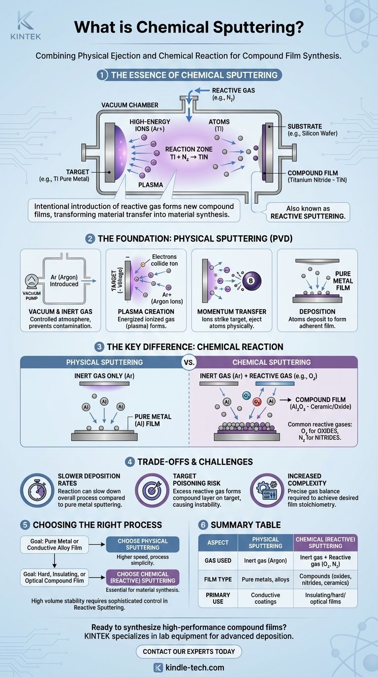
In essence, chemical sputtering is a thin-film deposition process that combines the physical ejection of atoms from a source with a deliberate chemical reaction to create a new compound material on a substrate. While all sputtering begins with a physical mechanism, the "chemical" part refers to the introduction of a reactive gas (like oxygen or nitrogen) into the vacuum chamber. This allows for the creation of films like ceramics and oxides, which is not possible with purely physical sputtering.
While all sputtering physically ejects atoms from a source target, chemical sputtering—more commonly known as reactive sputtering—intentionally introduces a reactive gas to form new compound films. This transforms the process from simple material transfer into material synthesis.
The Foundation: Understanding Physical Sputtering
To understand what makes chemical sputtering unique, you must first grasp the fundamentals of physical sputtering, which is the basis for all sputtering techniques.
The Core Principle: Momentum Transfer
Sputtering is a physical vapor deposition (PVD) process. It works by ejecting atoms from a solid material, called the target, by bombarding it with high-energy ions inside a vacuum.
This is not a thermal process like evaporation. Instead, it is a purely mechanical, momentum-transfer event, like a microscopic billiard ball collision.
The Vacuum Environment
The entire process takes place in a vacuum chamber that is first pumped down to remove air and then backfilled with a small amount of an inert gas, most commonly Argon (Ar).
This controlled atmosphere prevents contamination and allows for the creation of a stable plasma.
Creating the Plasma
A strong negative voltage is applied to the target material. This electrical field energizes free electrons, which then collide with the neutral Argon atoms.
These collisions knock electrons off the Argon atoms, turning them into positively charged Argon ions (Ar+). This energized, ionized gas is known as a plasma.
The Bombardment and Deposition Process
The positively charged Argon ions are forcefully accelerated toward the negatively charged target.
They strike the target with enough kinetic energy to dislodge, or "sputter," atoms from the target material. These sputtered atoms travel across the chamber and deposit onto the substrate (e.g., a silicon wafer or glass panel), forming a thin, highly adherent film.
The Key Difference: Introducing a Chemical Reaction
Chemical sputtering, or reactive sputtering, builds upon this physical foundation by adding one critical ingredient: a reactive gas.
What is a Reactive Gas?
Instead of using only an inert gas like Argon, a carefully controlled amount of a reactive gas is also fed into the chamber.
Common examples include Oxygen (O₂) to form oxide films or Nitrogen (N₂) to form nitride films.
How It Forms New Compounds
As atoms are physically sputtered from the pure metal target (e.g., Titanium), they travel through the plasma.
During this transit, or upon arrival at the substrate, they chemically react with the reactive gas. For example, a sputtered Titanium (Ti) atom will react with Nitrogen (N₂) to form a Titanium Nitride (TiN) film on the substrate—a hard, gold-colored ceramic.
This allows you to start with a simple, pure metal target and synthesize a completely different compound material as the final film.
Understanding the Trade-offs and Challenges
While powerful, reactive sputtering introduces complexities not found in purely physical processes.
Slower Deposition Rates
The chemical reaction process and the potential for the target to react with the gas can slow down the overall deposition rate compared to sputtering a pure metal in an inert atmosphere.
The Risk of Target Poisoning
If the reactive gas pressure is too high, the gas will begin to form a compound layer (e.g., an oxide or nitride) on the surface of the sputtering target itself.
This phenomenon, known as target poisoning, can drastically alter the electrical properties of the target, leading to an unstable process and poor film quality.
Increased Process Complexity
Successfully managing reactive sputtering requires sophisticated control over the partial pressures of both the inert and reactive gases. Maintaining the precise balance to achieve the desired film stoichiometry without poisoning the target is a significant engineering challenge.
Choosing the Right Sputtering Process
Your choice between physical and reactive sputtering depends entirely on the material you need to create.
- If your primary focus is depositing a pure metal or conductive alloy film: Stick with non-reactive physical sputtering (like DC or magnetron sputtering) for its higher speed and process simplicity.
- If your primary focus is creating a hard, insulating, or optically specific compound film (e.g., a ceramic, oxide, or nitride): Chemical (reactive) sputtering is the essential and correct choice for synthesizing the material during deposition.
- If your primary focus is process stability at high volumes: Be aware that reactive sputtering requires more sophisticated feedback and control systems to manage gas ratios and prevent target poisoning.
Ultimately, understanding the interplay between physical bombardment and chemical reaction empowers you to select the precise deposition method for your material's unique requirements.
Summary Table:
| Aspect | Physical Sputtering | Chemical (Reactive) Sputtering |
|---|---|---|
| Gas Used | Inert gas (Argon) | Inert gas + Reactive gas (O₂, N₂) |
| Film Type | Pure metals, alloys | Compounds (oxides, nitrides, ceramics) |
| Key Process | Physical momentum transfer | Physical ejection + Chemical reaction |
| Primary Use | Conductive coatings | Insulating/hard/optical films |
| Complexity | Simpler, faster deposition | Higher complexity, risk of target poisoning |
Ready to synthesize high-performance compound films? KINTEK specializes in lab equipment and consumables for advanced deposition processes like reactive sputtering. Whether you need to create durable nitride coatings or precise oxide layers, our expertise ensures optimal process stability and film quality. Contact our experts today to discuss how we can support your laboratory's thin-film synthesis needs!
Visual Guide