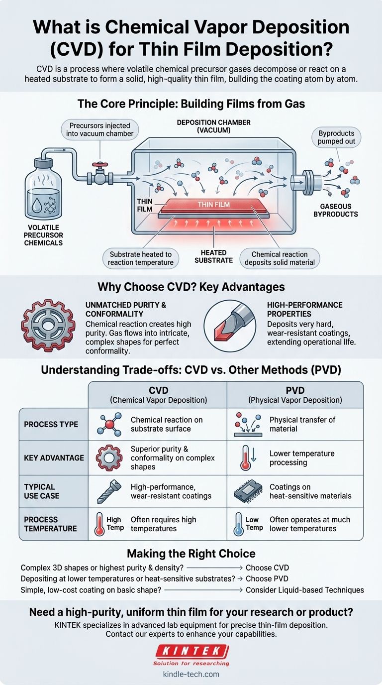
In essence, Chemical Vapor Deposition (CVD) is a process where volatile chemical precursors are introduced as a gas into a reaction chamber. These gases then decompose or react on the surface of a heated object, known as a substrate, to form a solid, high-quality thin film. The process builds the coating atom by atom, ensuring an even and highly controlled layer.
Unlike physical methods that simply transfer a source material onto a surface, CVD constructs a new film through a controlled chemical reaction. This chemical foundation is the key to its unique ability to create exceptionally pure, dense, and uniform coatings, even on complex shapes.
The Core Principle: Building Films from Gas
Chemical Vapor Deposition is a sophisticated technique used when the properties of the final film—such as purity, density, and uniformity—are critical. The process relies on a few key elements working in concert.
The Role of the Precursor
The process begins with one or more volatile precursor chemicals. These are compounds, often in liquid or solid form, that can be easily vaporized and contain the specific atoms required for the final film. This vapor is then precisely injected into the deposition chamber.
The Importance of Heat and Vacuum
The deposition chamber is typically held under a vacuum to remove air and other potential contaminants that could compromise the film's purity. The substrate inside the chamber is heated to a specific reaction temperature, which provides the necessary energy to trigger the chemical reaction.
The Deposition Mechanism
As the precursor gas flows over the heated substrate, it breaks down or reacts on the hot surface. This chemical reaction deposits the desired solid material directly onto the substrate, forming a thin film. Gaseous byproducts from the reaction are simply pumped out of the chamber, leaving behind an exceptionally pure coating. Over time, this process builds the film layer by layer.
Why Choose CVD? Key Advantages
CVD is chosen over other techniques when specific, high-performance characteristics are required that are difficult to achieve otherwise.
Unmatched Purity and Conformality
Because the film is built from a chemical reaction rather than a physical transfer, CVD can produce films with an extremely high degree of purity. Furthermore, since the precursor is a gas, it can flow into and coat intricate, complex three-dimensional surfaces with a perfectly uniform thickness, a property known as high conformality.
High-Performance Properties
The CVD process allows for the creation of films with unique and desirable characteristics. It is widely used to deposit very hard, wear-resistant coatings on cutting tools or industrial parts, significantly extending their operational life.
Understanding the Trade-offs: CVD vs. Other Methods
No single deposition method is perfect for every application. Understanding the trade-offs is key to making an informed decision. The primary alternative to CVD is Physical Vapor Deposition (PVD), which includes methods like sputtering and evaporation.
Chemical vs. Physical Process
The fundamental difference is in the name. CVD is a chemical process where a new material is formed on the substrate. PVD is a physical process where a source material is vaporized (e.g., by blasting it with ions) and then simply re-condenses on the substrate, much like steam condensing on a cold window.
Higher Process Temperatures
A significant trade-off of CVD is that it often requires high temperatures to drive the chemical reactions. This can limit the types of substrate materials that can be used, as some may not withstand the heat without being damaged or altered. PVD methods can often operate at much lower temperatures.
Precursor Complexity
CVD precursors can be complex, expensive, and sometimes hazardous chemicals that require careful handling and safety protocols. PVD, by contrast, often uses a solid, inert target material, which can be simpler and safer to manage.
Making the Right Choice for Your Goal
Selecting the right deposition method depends entirely on your project's specific requirements for film properties, substrate material, and component geometry.
- If your primary focus is coating complex 3D shapes or achieving the highest possible film purity and density: CVD is often the superior choice due to its gas-phase nature and chemical selectivity.
- If your primary focus is depositing materials at lower temperatures or on heat-sensitive substrates: Physical Vapor Deposition (PVD) methods like sputtering or evaporation may be more appropriate.
- If your goal is a simple, low-cost coating on a basic shape for a less demanding application: Simpler liquid-based techniques, such as the chemical bath method, could be a sufficient and more economical solution.
By understanding the fundamental mechanism of CVD, you can strategically leverage its chemical precision to build materials with unparalleled performance.
Summary Table:
| Aspect | CVD (Chemical Vapor Deposition) | PVD (Physical Vapor Deposition) |
|---|---|---|
| Process Type | Chemical reaction on substrate surface | Physical transfer of material |
| Key Advantage | Superior purity & conformality on complex shapes | Lower temperature processing |
| Typical Use Case | High-performance, wear-resistant coatings | Coatings on heat-sensitive materials |
Need a high-purity, uniform thin film for your research or product?
KINTEK specializes in providing advanced lab equipment and consumables for precise thin-film deposition. Our expertise in CVD technology can help you achieve the exceptional film purity, density, and conformality your project demands.
Contact our experts today to discuss how our solutions can enhance your laboratory's capabilities and drive your innovations forward.
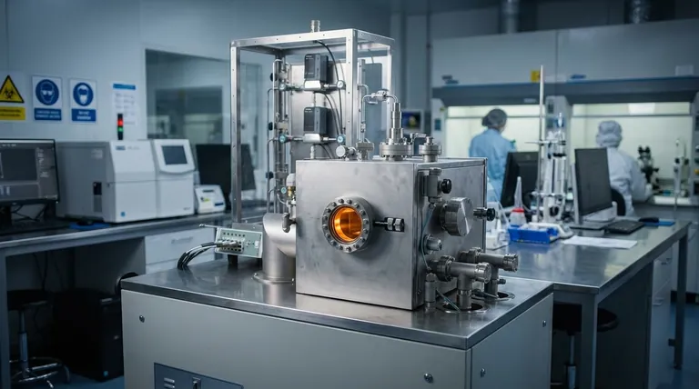
Visual Guide
Related Products
- Chemical Vapor Deposition CVD Equipment System Chamber Slide PECVD Tube Furnace with Liquid Gasifier PECVD Machine
- Microwave Plasma Chemical Vapor Deposition MPCVD Machine System Reactor for Lab and Diamond Growth
- 915MHz MPCVD Diamond Machine Microwave Plasma Chemical Vapor Deposition System Reactor
- Customer Made Versatile CVD Tube Furnace Chemical Vapor Deposition Chamber System Equipment
- HFCVD Machine System Equipment for Drawing Die Nano-Diamond Coating
People Also Ask
- What types of substrates are used in CVD to facilitate graphene films? Optimize Graphene Growth with the Right Catalyst
- How are carbon nanotubes grown? Master Scalable Production with Chemical Vapor Deposition
- What are the core advantages of PE-CVD in OLED encapsulation? Protect Sensitive Layers with Low-Temp Film Deposition
- What are the processes of vapor phase deposition? Understand CVD vs. PVD for Superior Thin Films
- What is the chemical vapor deposition growth process? Build Superior Thin Films from the Atom Up


