At its core, Chemical Vapor Deposition (CVD) is a highly versatile manufacturing process used to create high-purity, high-performance solid materials. It functions by depositing a thin film from a gaseous state onto a solid substrate, making it fundamental to industries ranging from semiconductors and electronics to medical devices and advanced tools.
The true value of CVD lies not just in coating surfaces, but in its ability to build materials atom-by-atom from a chemical reaction. This provides an unparalleled level of control over purity, structure, and performance, enabling the creation of materials that would otherwise be impossible to fabricate.
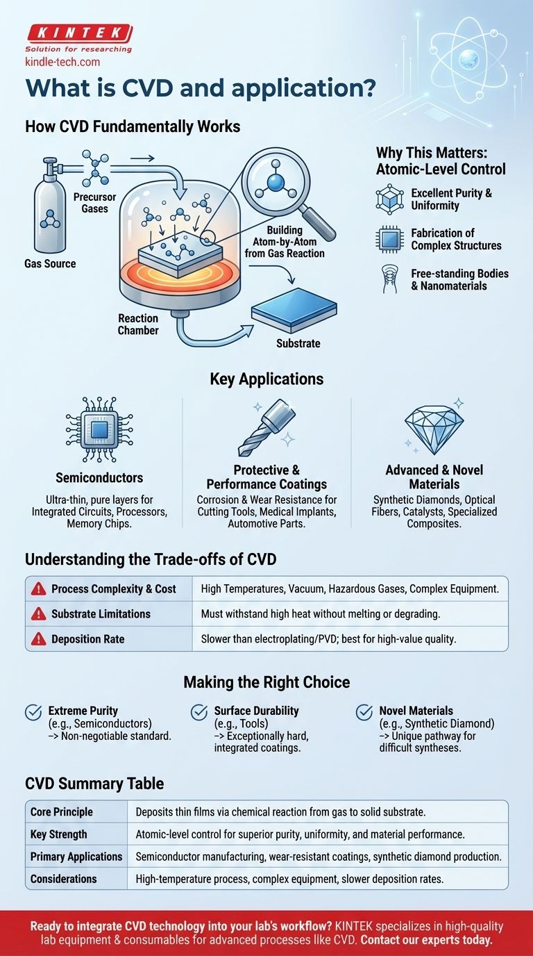
How CVD Fundamentally Works
The Core Principle: Building from Gas
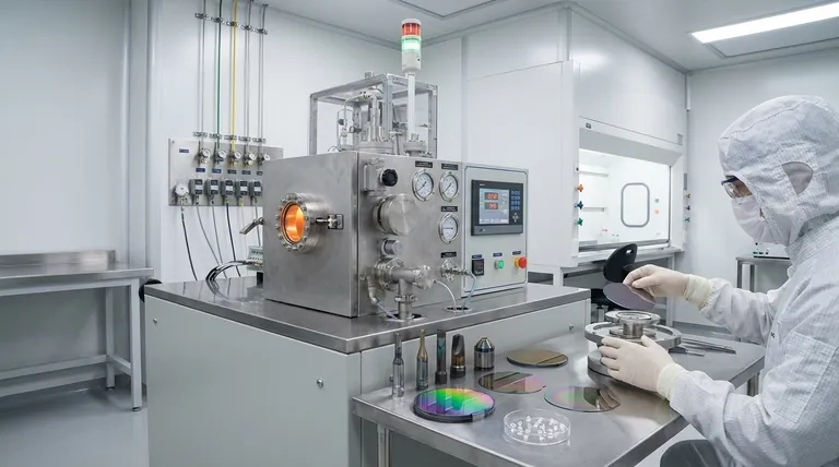
CVD involves introducing precursor gases into a reaction chamber containing the object to be coated, known as the substrate.
When these gases come into contact with the heated substrate, a chemical reaction is triggered. This reaction causes a solid material to form and deposit onto the substrate's surface, creating a thin, solid film.
Think of it as a highly controlled and precise version of frost forming on a cold windowpane, but instead of water vapor freezing, specific chemicals are reacting to build a new material layer.
Why This Matters: Atomic-Level Control
Because CVD is a chemical process rather than a physical one (like spraying paint), it yields materials with excellent purity and uniformity.
This precise control allows for the fabrication of complex, high-performance structures. It is used not only to apply coatings but also to create free-standing bodies, powders, filaments, and even intricate nanomaterials.
Key Applications: From Microchips to Medical Implants
The Semiconductor Industry
CVD is the bedrock technology for manufacturing modern electronics. It is used to deposit the ultra-thin, exceptionally pure layers of insulating, conducting, and semiconducting materials that form integrated circuits.
The process's ability to create uniform films over large areas is critical for producing microprocessors, memory chips, and other essential electronic components.
Protective and Performance Coatings
CVD is widely used to enhance the surface properties of tools and components, imparting significant corrosion and wear resistance.
Applications include coatings on machine tools for cutting, medical implants for biocompatibility and durability, and automotive parts for longevity. These coatings are not just layered on top; they are chemically bonded, making them incredibly robust.
Advanced and Novel Materials
The versatility of CVD extends to creating entirely new materials with unique properties.
Its most famous application in this area is the production of synthetic diamonds for industrial and electronic uses. It is also used to manufacture optical fibers, catalysts, and specialized composites that demand high performance.
Understanding the Trade-offs of CVD
Process Complexity and Cost
CVD processes often require high temperatures and vacuum conditions, making the equipment complex and expensive.
The precursor gases used can also be hazardous and require careful handling, adding to the operational overhead compared to simpler coating methods.
Substrate Limitations
The high temperatures required for many CVD reactions limit the types of materials that can be coated. Substrates must be able to withstand the heat without melting, deforming, or degrading.
Deposition Rate
While capable of producing superior quality films, CVD can be a slower process compared to bulk coating techniques like electroplating or physical vapor deposition (PVD). This makes it best suited for high-value applications where quality is more important than speed.
Making the Right Choice for Your Goal
When considering CVD, your decision should be guided by the specific material properties you need to achieve.
- If your primary focus is extreme purity and atomic-level control (e.g., semiconductors): CVD is often the non-negotiable standard due to its unmatched chemical precision.
- If your primary focus is enhancing surface durability (e.g., wear-resistant tools): CVD provides exceptionally hard and integrated coatings that dramatically extend a component's life.
- If your primary focus is creating novel materials with unique structures (e.g., synthetic diamond): CVD offers a unique pathway to synthesize materials that are difficult or impossible to form by other means.
Ultimately, CVD is an enabling technology that gives engineers and scientists the power to design and build materials from the ground up.
Summary Table:
| Feature | Key Aspect |
|---|---|
| Core Principle | Deposits thin films via chemical reaction from gas to solid substrate. |
| Key Strength | Atomic-level control for superior purity, uniformity, and material performance. |
| Primary Applications | Semiconductor manufacturing, wear-resistant coatings, synthetic diamond production. |
| Considerations | High-temperature process, complex equipment, slower deposition rates. |
Ready to integrate CVD technology into your lab's workflow?
KINTEK specializes in providing the high-quality lab equipment and consumables necessary for advanced processes like Chemical Vapor Deposition. Whether you are developing next-generation semiconductors, enhancing tool durability, or creating novel materials, we have the solutions to support your precision and performance goals.
Contact our experts today to discuss how we can equip your laboratory for success.
Visual Guide
Related Products
- CVD Diamond Dressing Tools for Precision Applications
- Multi Heating Zones CVD Tube Furnace Machine Chemical Vapor Deposition Chamber System Equipment
- CVD Diamond Domes for Industrial and Scientific Applications
- CVD Diamond for Thermal Management Applications
- Chemical Vapor Deposition CVD Equipment System Chamber Slide PECVD Tube Furnace with Liquid Gasifier PECVD Machine
People Also Ask
- What are the raw materials for CVD diamonds? A seed, a gas, and the science of crystal growth.
- How long does it take to make synthetic diamonds? Discover the 6-8 Week Science Behind Lab-Grown Gems
- What are the disadvantages of CVD diamonds? Understanding the trade-offs for your purchase.
- What is chemical vapor deposition of diamond? Grow High-Purity Diamonds Atom-by-Atom
- Can CVD diamonds change color? No, their color is permanent and stable.


