In essence, Chemical Vapor Deposition (CVD) is a highly controlled, bottom-up manufacturing process used to create high-purity, high-performance nanomaterials and thin films. It works by introducing reactive gases into a chamber where they decompose on a heated surface, known as a substrate, to form a solid deposit. This method allows for the creation of materials like graphene, carbon nanotubes, and synthetic diamonds with atomic-level precision.
At its core, CVD is a technique for building materials atom by atom. It offers exceptional control over a material's purity, structure, and thickness, making it a versatile and scalable choice for advanced nanofabrication.
How the CVD Process Works at the Nanoscale
The CVD process might seem complex, but it operates on a set of fundamental principles involving heat, chemistry, and a controlled environment.
The Core Components
The process takes place inside a reaction chamber. Key elements include a substrate, which is the material upon which the new film will grow, gaseous reactants (precursors), and a heat source. Carrier gases are often used to transport the reactants into the chamber.
The Deposition Sequence
First, precursor gases containing the required elements are introduced into the chamber. The substrate is then heated to a specific, critical temperature.
When the hot gases make contact with the substrate, a chemical reaction is triggered. This reaction causes a solid material to deposit onto the substrate surface, forming a thin, uniform film or discrete nanostructures. Waste gases are then pumped out of the chamber.
The Role of the Substrate and Catalyst
The substrate is not merely a passive surface. For many nanomaterials, such as graphene or carbon nanotubes, the substrate (often a metal like copper or iridium) acts as a catalyst.
The catalyst serves two functions: it helps break down the precursor gases and provides an active surface for the nucleation and growth of the nanomaterial's lattice structure.
Key Advantages of Using CVD for Nanomaterials
CVD has become a cornerstone of nanofabrication due to several distinct advantages that set it apart from other methods.
Atomic-Level Precision and Purity
CVD excels at creating chemically bonded thin films with excellent uniformity and purity. Because it builds materials from the gas phase, it's possible to control film thickness and composition at the atomic level, minimizing impurities like metallic inclusions.
Versatility Across Materials
The process is exceptionally versatile. It is used extensively to synthesize a wide range of carbon-based nanomaterials, including graphene, fullerenes, and carbon nanotubes (CNTs). It is also a leading method for producing large-area, high-clarity lab-grown diamonds.
Scalability and Production Rate
Compared to many nanofabrication techniques, CVD is relatively fast and can be scaled to produce materials over large areas, such as coating entire semiconductor wafers. This makes it suitable for both research and high-volume industrial production.
Control Over Final Structure
The final material's microstructure and properties are highly controllable. The substrate temperature is the most critical parameter, as it directly defines the type and rate of the chemical reaction, influencing the final film's characteristics.
Understanding the Trade-offs and Considerations
While powerful, the CVD method is not without its challenges. An objective assessment requires understanding its limitations.
Process Sensitivity
The high quality of CVD films is directly tied to a high degree of process control. Factors like temperature, pressure, and gas flow rates must be precisely managed, as even small deviations can significantly impact the final material's quality and uniformity.
Substrate Compatibility and Transfer
For applications where the nanomaterial is needed on a different surface (e.g., placing graphene on a transparent polymer), a transfer process is required. This step involves separating the film from the growth substrate, which can introduce defects, tears, or contamination if not performed carefully.
Precursor and Equipment Factors
While setup costs can be lower than some ultra-high-pressure alternatives (like HPHT for diamonds), CVD equipment is still a significant investment. Furthermore, the precursor gases can be expensive, toxic, or flammable, requiring specialized handling and safety protocols.
Making the Right Choice for Your Goal
Selecting CVD depends entirely on your project's specific requirements for material quality, scale, and complexity.
- If your primary focus is producing high-purity, large-area films like graphene or diamond: CVD is an ideal choice due to its proven scalability and control over film uniformity and purity.
- If your primary focus is creating complex crystalline layers for semiconductors: Specialized versions of CVD, such as Metal-Organic CVD (MOCVD), are the established industry standard for this exact purpose.
- If your primary focus is material performance over process simplicity: CVD is a superior option when the precision, purity, and structural integrity of the nanomaterial are more critical than the initial setup cost or process complexity.
By understanding its principles and trade-offs, you can leverage CVD to engineer materials with precision from the atom up.
Summary Table:
| Aspect | Description |
|---|---|
| Process | Bottom-up fabrication using gas-phase reactions on a heated substrate. |
| Key Materials | Graphene, Carbon Nanotubes (CNTs), Synthetic Diamonds, Thin Films. |
| Primary Advantage | Exceptional control over purity, structure, and thickness at the atomic level. |
| Key Consideration | Requires precise control of temperature, pressure, and gas flow for high-quality results. |
Ready to Engineer Advanced Nanomaterials with Precision?
Chemical Vapor Deposition is a powerful technique for creating high-performance materials, but it requires reliable equipment and expert support. KINTEK specializes in providing the lab equipment and consumables that researchers and manufacturers need to perfect their CVD processes.
Whether you are scaling up graphene production or developing next-generation semiconductor films, we have the solutions to support your goals. Contact our experts today to discuss how we can help you achieve superior material quality and process efficiency.
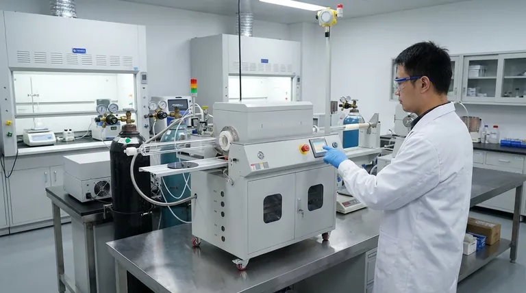
Visual Guide

Related Products
- Chemical Vapor Deposition CVD Equipment System Chamber Slide PECVD Tube Furnace with Liquid Gasifier PECVD Machine
- Customer Made Versatile CVD Tube Furnace Chemical Vapor Deposition Chamber System Equipment
- HFCVD Machine System Equipment for Drawing Die Nano-Diamond Coating
- Split Chamber CVD Tube Furnace with Vacuum Station Chemical Vapor Deposition System Equipment Machine
- Multi Heating Zones CVD Tube Furnace Machine Chemical Vapor Deposition Chamber System Equipment
People Also Ask
- Why is Chemical Vapor Deposition (CVD) equipment uniquely suited for constructing hierarchical superhydrophobic structures?
- What types of substrates are used in CVD to facilitate graphene films? Optimize Graphene Growth with the Right Catalyst
- What are the advantages of chemical vapor deposition? Achieve Superior Thin Films for Your Lab
- What are the core advantages of PE-CVD in OLED encapsulation? Protect Sensitive Layers with Low-Temp Film Deposition
- How are carbon nanotubes grown? Master Scalable Production with Chemical Vapor Deposition


