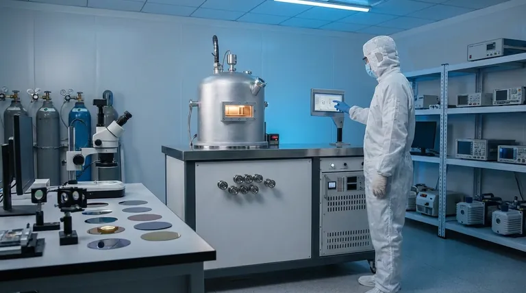
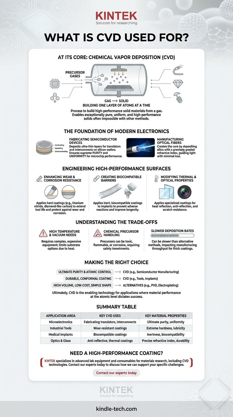
At its core, Chemical Vapor Deposition (CVD) is a process used to build high-performance solid materials from a gas. Its most common applications involve depositing exceptionally pure, thin films for the semiconductor industry and creating incredibly durable, functional coatings for industrial and medical components. This versatility makes it essential for manufacturing everything from computer chips and optical fibers to artificial diamonds and biomedical implants.
The true value of CVD lies in its precision. By building materials one layer of atoms at a time from a chemical gas, it enables the creation of exceptionally pure, uniform, and high-performance solids that are often impossible to produce with conventional melting or machining methods.
The Foundation of Modern Electronics
CVD is the backbone of the microelectronics industry. Its ability to create flawless, ultra-thin layers of material is fundamental to fabricating the complex structures found in modern integrated circuits.
Fabricating Semiconductor Devices
CVD is used to deposit the various layers—conducting, insulating, and semiconducting—that form the transistors and interconnects on a silicon wafer. The process ensures supreme purity and uniformity, which are critical for the electrical performance and reliability of a microchip.
Manufacturing Optical Fibers
The process is also used to create the core of optical fibers. By carefully controlling the mixture of gases, manufacturers use CVD to deposit layers of silica with a precisely graded refractive index, which is what guides light signals over long distances with minimal loss.
Engineering High-Performance Surfaces
Beyond electronics, CVD is a dominant technology for enhancing the surface properties of materials. It creates coatings that are chemically bonded to the substrate, resulting in exceptional adhesion and durability.
Enhancing Wear and Corrosion Resistance
CVD is used to apply hard coatings like titanium nitride or diamond-like carbon onto machine tools, engine components, and cutting blades. These layers dramatically increase hardness and lubricity, extending the life of the tool and protecting it from corrosion and wear.
Creating Biocompatible Barriers
In the medical field, CVD applies inert, biocompatible coatings to implants like stents and artificial joints. These coatings prevent adverse reactions with the body and can improve the device's longevity and performance.
Modifying Thermal and Optical Properties
The process is used to apply specialized coatings to glass. These can range from heat-reflective layers on architectural windows to anti-reflective coatings on lenses and scratch-resistant layers on consumer electronics.
Understanding the Trade-offs
While powerful, CVD is not a universal solution. Understanding its limitations is key to deciding if it is the right process for a given application.
High Temperature and Vacuum Needs
Most CVD processes require high temperatures and a high-vacuum environment. This necessitates complex, expensive equipment and can limit the types of substrate materials that can be coated without being damaged by heat.
Chemical Precursor Handling
The gases used as precursors in CVD can be highly toxic, flammable, or corrosive. This requires significant investment in safety systems, gas handling infrastructure, and waste abatement.
Slower Deposition Rates
Compared to some alternative methods like Physical Vapor Deposition (PVD), CVD can have a slower rate of material deposition. For applications where thick coatings are needed quickly, this can impact manufacturing throughput and cost.
Making the Right Choice for Your Goal
Selecting a manufacturing process depends entirely on the required material properties and economic constraints.
- If your primary focus is ultimate purity and atomic-level control: CVD is the definitive choice for applications like semiconductor manufacturing, where flawless crystal structures are non-negotiable.
- If your primary focus is a durable, conformal coating on a complex shape: CVD excels at uniformly coating intricate surfaces, making it ideal for tools, implants, and components that need complete protection.
- If your primary focus is high-volume, low-cost coating on a simple shape: You should evaluate simpler alternatives like PVD or electroplating, as the complexity and cost of CVD may not be justified.
Ultimately, CVD is the enabling technology for applications where material performance at the atomic level dictates success.
Summary Table:
| Application Area | Key CVD Uses | Key Material Properties |
|---|---|---|
| Microelectronics | Fabricating transistors, interconnects on silicon wafers | Ultimate purity, uniformity, atomic-level control |
| Industrial Tools | Wear-resistant coatings (e.g., titanium nitride) on cutting blades | Extreme hardness, lubricity, corrosion resistance |
| Medical Implants | Biocompatible coatings on stents and artificial joints | Inertness, biocompatibility, improved longevity |
| Optics & Glass | Anti-reflective, scratch-resistant, or thermal coatings | Precise refractive index, durability, functionality |
Need to deposit a high-performance, ultra-pure, or durable coating?
KINTEK specializes in providing advanced lab equipment and consumables for materials research and development, including technologies like CVD. Whether you are developing next-generation semiconductors, enhancing industrial tool life, or creating biocompatible medical devices, our solutions can help you achieve the precise material properties you need.
Contact our experts today to discuss how we can support your specific laboratory and manufacturing challenges.
Visual Guide
Related Products
- CVD Diamond Dressing Tools for Precision Applications
- Multi Heating Zones CVD Tube Furnace Machine Chemical Vapor Deposition Chamber System Equipment
- CVD Diamond Domes for Industrial and Scientific Applications
- CVD Diamond for Thermal Management Applications
- Chemical Vapor Deposition CVD Equipment System Chamber Slide PECVD Tube Furnace with Liquid Gasifier PECVD Machine
People Also Ask
- Can CVD diamonds change color? No, their color is permanent and stable.
- What is chemical vapor deposition of diamond? Grow High-Purity Diamonds Atom-by-Atom
- What is CVD diamond? The Ultimate Guide to Lab-Grown Diamonds and Their Uses
- Does the chemical vapor deposition be used for diamonds? Yes, for Growing High-Purity Lab Diamonds
- How do you identify a CVD diamond? The Definitive Guide to Lab-Grown Diamond Verification


