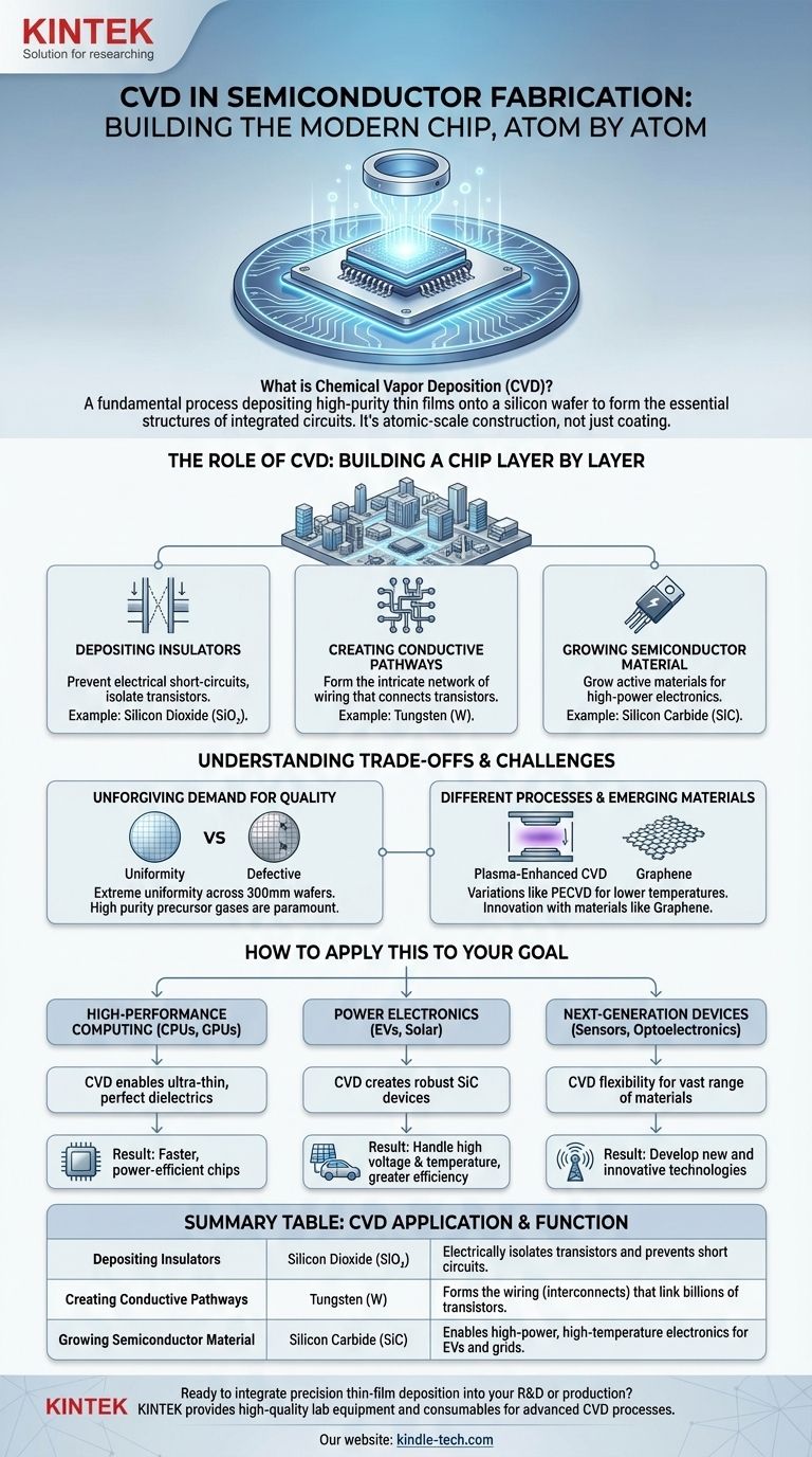
In short, Chemical Vapor Deposition (CVD) is used in the semiconductor industry to build the microscopic layers that make up a modern chip. It is a fundamental fabrication process that deposits a wide variety of high-purity thin films onto a silicon wafer. These films can be insulating, conductive, or semiconducting, forming the essential structures of transistors, interconnects, and other integrated circuit components.
The core problem CVD solves is not just depositing a material, but doing so with the extreme precision and purity required to construct functional electronic devices with billions of components on a surface the size of a fingernail. It is less like coating and more like atomic-scale construction.
The Role of CVD: Building a Chip Layer by Layer
A modern integrated circuit is a three-dimensional metropolis of microscopic components. CVD is the primary construction method used to build up the "floors" and "wiring" of this city on the surface of a silicon wafer.
What is Chemical Vapor Deposition?
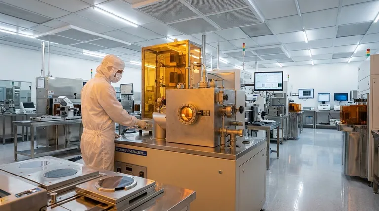
At its heart, CVD is a process where a wafer (the substrate) is placed in a reaction chamber and exposed to one or more volatile precursor gases. These gases react or decompose on the wafer's hot surface, forming a solid, stable thin film of the desired material. Any excess gas or volatile byproducts are then pumped out of the chamber.
Depositing Insulators: Preventing Microscopic Chaos
One of the most critical uses of CVD is to deposit insulating films, often made of silicon dioxide or silicon nitride. In an integrated circuit with billions of transistors packed together, these insulating layers are essential.
They prevent electrical short-circuits between the microscopic metal wires (interconnects) and electrically isolate one transistor from another, ensuring signals go only where they are intended. An example is depositing phosphosilicate glass (PSG) for encapsulation, which protects the final chip.
Creating Conductive Pathways: Wiring the Circuit
CVD is also used to deposit metallic materials, such as tungsten or copper. These layers form the intricate network of conductive pathways—the "wiring"—that connects the millions or billions of transistors together, allowing them to communicate and perform logical operations.
Growing the Semiconductor Material Itself
In some applications, CVD is used to grow the active semiconductor material. For example, it's used to grow high-purity crystalline silicon or specialized materials like silicon carbide (SiC). These SiC films are crucial for high-power electronics used in electric vehicles and advanced power grids because they can handle much higher voltages and temperatures than traditional silicon.
Understanding the Trade-offs and Challenges
While CVD is a cornerstone of manufacturing, it is not without its complexities. The success of the entire chip fabrication process often hinges on how well the CVD steps are controlled.
The Unforgiving Demand for Quality
The films deposited by CVD must be incredibly uniform across the entire wafer, which can be up to 300mm (12 inches) in diameter. Any imperfection, pinhole, or particle of dust can create a defect that renders a chip useless. The purity of the precursor gases is paramount.
Different Processes for Different Needs
There are multiple variations of CVD, each with its own advantages. For instance, Plasma-Enhanced CVD (PECVD) uses a plasma to assist the chemical reaction. This allows deposition to occur at lower temperatures, which is critical for preventing damage to layers that have already been built on the wafer in previous steps.
Emerging Applications and Materials
The versatility of CVD keeps it at the forefront of innovation. Researchers are using it to produce high-quality films of novel materials like graphene, a single-atom-thick layer of carbon. Graphene's unique properties hold immense promise for future applications in ultra-fast electronics, highly sensitive sensors, and energy storage.
How to Apply This to Your Goal
The specific importance of CVD depends entirely on the desired outcome of the final semiconductor device.
- If your primary focus is high-performance computing (CPUs, GPUs): CVD's ability to deposit ultra-thin, perfect insulating layers (dielectrics) is what allows transistors to be packed closer together, making chips faster and more power-efficient.
- If your primary focus is power electronics (EVs, solar inverters): CVD is essential for creating robust silicon carbide (SiC) devices that can withstand extreme operating conditions, enabling greater efficiency and reliability.
- If your primary focus is next-generation devices (sensors, optoelectronics): CVD's flexibility in depositing a vast range of materials, including polymers and 2D materials like graphene, is the key to developing new and innovative technologies.
Ultimately, Chemical Vapor Deposition is the foundational process that transforms a blank silicon wafer into a complex and powerful electronic brain.
Summary Table:
| CVD Application | Material Example | Function in Semiconductor |
|---|---|---|
| Depositing Insulators | Silicon Dioxide (SiO₂) | Electrically isolates transistors and prevents short circuits. |
| Creating Conductive Pathways | Tungsten (W) | Forms the wiring (interconnects) that link billions of transistors. |
| Growing Semiconductor Material | Silicon Carbide (SiC) | Enables high-power, high-temperature electronics for EVs and grids. |
Ready to integrate precision thin-film deposition into your semiconductor R&D or production? KINTEK specializes in providing high-quality lab equipment and consumables for advanced CVD processes. Whether you are developing next-generation computing chips, robust power electronics, or innovative sensors, our solutions support the extreme purity and uniformity your work demands. Contact our experts today to discuss how we can help you achieve your fabrication goals.
Visual Guide
Related Products
- Chemical Vapor Deposition CVD Equipment System Chamber Slide PECVD Tube Furnace with Liquid Gasifier PECVD Machine
- Customer Made Versatile CVD Tube Furnace Chemical Vapor Deposition Chamber System Equipment
- Microwave Plasma Chemical Vapor Deposition MPCVD Machine System Reactor for Lab and Diamond Growth
- 915MHz MPCVD Diamond Machine Microwave Plasma Chemical Vapor Deposition System Reactor
- Multi Heating Zones CVD Tube Furnace Machine Chemical Vapor Deposition Chamber System Equipment
People Also Ask
- What types of substrates are used in CVD to facilitate graphene films? Optimize Graphene Growth with the Right Catalyst
- How are carbon nanotubes grown? Master Scalable Production with Chemical Vapor Deposition
- What are the advantages of chemical vapor deposition? Achieve Superior Thin Films for Your Lab
- What are the core advantages of PE-CVD in OLED encapsulation? Protect Sensitive Layers with Low-Temp Film Deposition
- What is the chemical vapor deposition growth process? Build Superior Thin Films from the Atom Up


