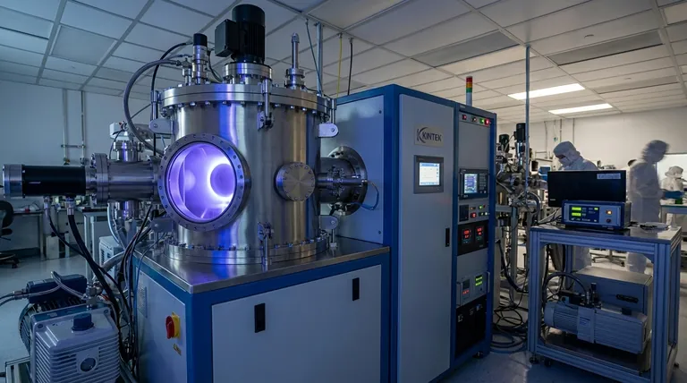
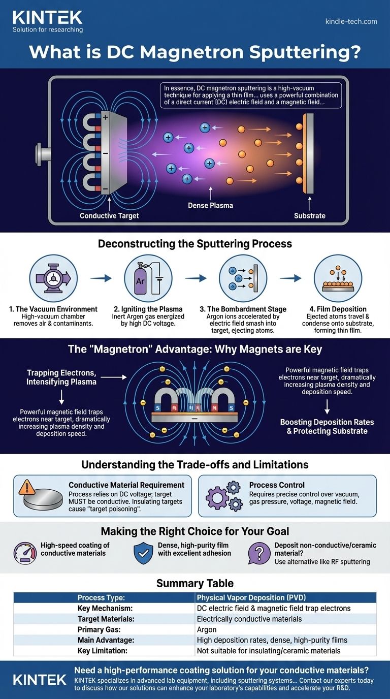
In essence, DC magnetron sputtering is a high-vacuum technique for applying a thin film of material onto a surface. It uses a powerful combination of a direct current (DC) electric field and a magnetic field to create a concentrated gas plasma. This plasma bombards a source material, known as the "target," dislodging atoms that then travel and deposit onto a substrate, forming a uniform, high-quality coating.
The core challenge in any sputtering process is generating enough ions to efficiently coat a surface. DC magnetron sputtering solves this by using a specially configured magnetic field to trap electrons near the target, creating a dense, supercharged plasma that dramatically increases the speed and efficiency of the deposition.

Deconstructing the Sputtering Process
To understand how DC magnetron sputtering works, it's best to break it down into its fundamental stages. Each step plays a critical role in the final quality of the thin film.
The Vacuum Environment
The entire process must take place inside a high-vacuum chamber. Removing air and other contaminants is essential to ensure the purity of the final film and allow the sputtered atoms to travel unimpeded from the target to the substrate.
Igniting the Plasma
A low-pressure, inert gas (most commonly argon) is introduced into the chamber. A high DC voltage is then applied, creating a strong electric field between two electrodes: the cathode (the target material, which is negatively charged) and the anode.
This voltage energizes the argon gas, stripping electrons from the argon atoms. This creates a mixture of positively charged argon ions and free electrons, forming a visible plasma often called a "glow discharge."
The Bombardment Stage
The positively charged argon ions are powerfully accelerated by the electric field and smash into the negatively charged target surface. This high-energy collision has a physical impact, much like a sandblaster, that ejects or "sputters" individual atoms from the target material.
Film Deposition
These newly liberated atoms from the target travel through the vacuum chamber. They eventually strike the surface of the object being coated (the substrate), where they condense and build up, layer by layer, to form a thin, solid film.
The "Magnetron" Advantage: Why Magnets are Key
Standard sputtering works, but it can be slow and inefficient. The addition of a magnetic field—the "magnetron" part—revolutionizes the process.
Trapping Electrons, Intensifying Plasma
A powerful magnetic field is placed behind the target. This field acts like a magnetic fence, confining the lightweight, negatively charged electrons to a cyclical path very close to the target's surface.
Without this magnetic field, the electrons would quickly fly off to the anode. By trapping them, the magnetron dramatically increases the probability that these electrons will collide with and ionize more neutral argon atoms.
Boosting Deposition Rates
This enhanced ionization creates a much denser, more intense plasma concentrated directly in front of the target. With more argon ions available to bombard the target, the rate of sputtering increases significantly, leading to much faster film deposition.
Protecting the Substrate
The magnetic trap also prevents high-energy electrons from bombarding the substrate. This reduces heat load and potential damage, making the process suitable for more sensitive materials like plastics.
Understanding the Trade-offs and Limitations
While powerful, DC magnetron sputtering is not a universal solution. Its primary mechanism imposes a critical limitation.
The Conductive Material Requirement
Because the process relies on a DC voltage, the target material itself must be electrically conductive. A negative charge must be maintained on the target to attract the positive argon ions.
If you attempt to use an insulating or ceramic target, positive charge from the argon ions would quickly build up on its surface. This buildup, known as "target poisoning," effectively neutralizes the negative bias and shuts down the sputtering process.
Process Control
Achieving a high-quality, repeatable film requires precise control over multiple variables. Factors like vacuum level, gas pressure, voltage, and the strength and shape of the magnetic field all interact and must be carefully managed.
Making the Right Choice for Your Goal
Based on its mechanics, DC magnetron sputtering is the optimal choice for specific applications.
- If your primary focus is high-speed coating of conductive materials: DC magnetron sputtering is one of the most efficient and widely used industrial methods for depositing metals, alloys, and transparent conductive oxides.
- If your goal is a dense, high-purity film with excellent adhesion: The energetic nature of the sputtered atoms creates exceptionally high-quality functional coatings that bond well to the substrate.
- If you need to deposit a non-conductive or ceramic material: You must use an alternative, such as RF (Radio Frequency) sputtering, which is specifically designed to work with insulating targets.
By leveraging a magnetic field to supercharge a plasma, DC magnetron sputtering provides a fast, reliable, and high-quality method for advanced thin-film deposition.
Summary Table:
| Aspect | Key Detail |
|---|---|
| Process Type | Physical Vapor Deposition (PVD) |
| Key Mechanism | DC electric field & magnetic field trap electrons |
| Target Materials | Electrically conductive materials (metals, alloys) |
| Primary Gas | Argon |
| Main Advantage | High deposition rates and dense, high-purity films |
| Key Limitation | Not suitable for insulating/ceramic materials |
Need a high-performance coating solution for your conductive materials?
KINTEK specializes in advanced lab equipment, including sputtering systems, to meet your precise thin-film deposition needs. Our expertise ensures you get the right technology for high-speed, high-quality coatings with excellent adhesion.
Contact our experts today via our form to discuss how our solutions can enhance your laboratory's capabilities and accelerate your research and development.
Visual Guide

Related Products
People Also Ask
- What are the fundamentals of spark plasma sintering process? Unlock Rapid, High-Performance Material Consolidation
- What is SPS sintering method? A Guide to High-Speed, High-Performance Material Fabrication
- What is the mechanism of SPS process? A Deep Dive into Rapid, Low-Temperature Sintering
- Why are Spark Plasma Sintering (SPS) furnaces or hot presses utilized in the preparation of Li3PS4 solid electrolytes?
- What is the theory of spark plasma sintering? A Guide to Rapid, Low-Temperature Densification
