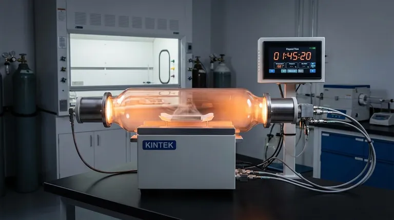
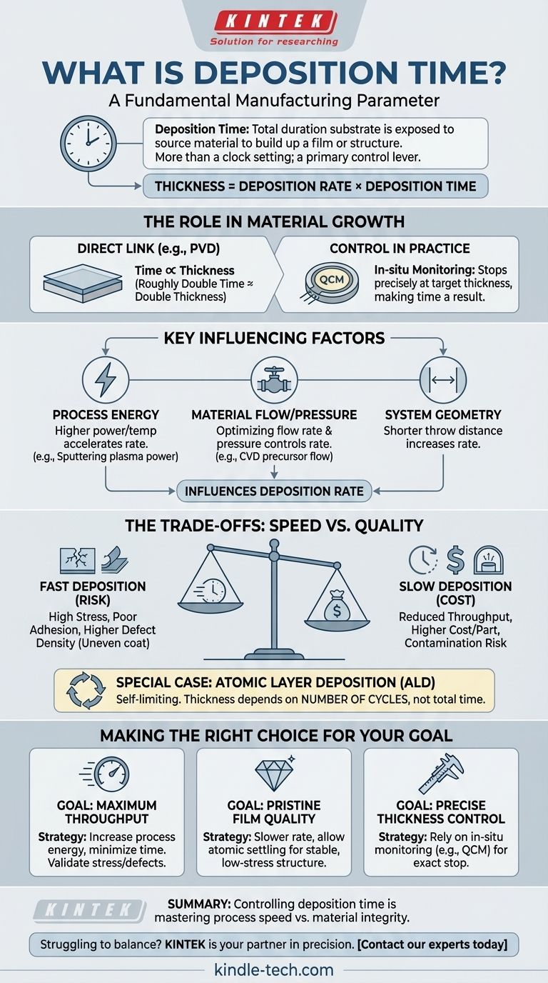
In any process where material is added to a surface, deposition time is the total duration that a substrate is exposed to the source material to build up a film or structure. This time is one of the most fundamental parameters in manufacturing, as it directly correlates with the amount of material deposited and, therefore, the final thickness and properties of the created layer.
Deposition time is more than a clock setting; it is a primary control lever for balancing manufacturing speed against final product quality. Understanding this trade-off is the key to mastering any thin-film or additive manufacturing process.
The Role of Deposition Time in Material Growth
Deposition time is a simple concept with deep implications for process control. It is rarely considered in isolation.
The Direct Link to Thickness
In most deposition processes, such as Physical Vapor Deposition (PVD), the relationship between time and thickness is straightforward. If you double the deposition time while holding all other parameters constant, you will roughly double the thickness of your film.
From Time to Growth Rate
Engineers and scientists more frequently discuss deposition rate (or growth rate). This is the crucial metric that connects time to a physical outcome.
The relationship is simple: Thickness = Deposition Rate × Deposition Time.
Rates are typically measured in units like nanometers per minute (nm/min) or Angstroms per second (Å/s). By characterizing the rate, you can pre-calculate the time needed to achieve a target thickness.
How It's Controlled in Practice
In a production environment, simply relying on a timer is often insufficient. High-precision processes use in-situ monitoring tools, such as a Quartz Crystal Microbalance (QCM), which measures the accumulated mass in real-time. The process is then stopped by the controller precisely when the target thickness is reached, making time a result rather than an input.
Key Factors That Influence Deposition Rate
The time required to deposit a specific thickness is not a constant. It is a function of the deposition rate, which is influenced by several key process parameters.
Process Energy
Higher energy input typically results in a faster deposition rate. In sputtering, this means increasing the plasma power. In thermal evaporation, it means raising the temperature of the source material. This accelerates the rate at which atoms are ejected from the source and travel to the substrate.
Material Flow and Pressure
The availability of the source material is fundamental. In Chemical Vapor Deposition (CVD), increasing the flow rate of the precursor gas can increase the growth rate. In PVD, the pressure of the inert gas (like Argon) affects the efficiency of the plasma and how easily material can travel to the substrate.
System Geometry
The physical arrangement of the deposition chamber—specifically the distance and angle between the material source and the substrate—has a significant impact. A shorter "throw distance" generally leads to a higher deposition rate at the cost of film uniformity across a large substrate.
Understanding the Trade-offs: Speed vs. Quality
Optimizing deposition time is a classic engineering balancing act. The shortest time is rarely the best time.
The Risk of Fast Deposition
Attempting to reduce deposition time by aggressively increasing the rate can be detrimental to quality. Fast-arriving atoms have less time and energy to find their ideal, low-energy positions in the crystal lattice.
This can lead to:
- High Internal Stress: Causing films to crack or delaminate.
- Poor Adhesion: The film may not stick well to the substrate.
- Higher Defect Density: Resulting in a more porous, less ordered structure with inferior electrical or optical properties.
Think of it like painting a wall too quickly; you get an uneven coat with drips and imperfections.
The Cost of Slow Deposition
Conversely, an excessively long deposition time, while often producing higher-quality films, has direct economic consequences. It reduces equipment throughput, increases the cost per part, and raises the risk of unintended contamination from residual gases in the vacuum chamber over a longer period.
The Special Case: Atomic Layer Deposition (ALD)
ALD is a unique process where growth is self-limiting. The substrate is exposed to precursor gases in discrete, sequential cycles. During each cycle, only one atomic layer (or a fraction of one) can form.
In ALD, increasing the exposure time beyond the point of saturation does not increase the thickness. The total deposition time is therefore determined by the number of cycles, not the duration of any single step.
Making the Right Choice for Your Goal
The ideal deposition time is not a single number; it is a function of your specific objective.
- If your primary focus is maximum throughput: You will aim for the shortest deposition time by increasing process energy, but you must validate that film stress and defectivity remain within acceptable limits.
- If your primary focus is pristine film quality: You will likely use a slower deposition rate, allowing atoms more time to settle into a stable, low-stress structure.
- If your primary focus is precise thickness control: You will rely on in-situ monitoring tools to stop the process at the exact moment the target thickness is reached, rather than relying on a pre-set time.
Ultimately, controlling deposition time is about mastering the fundamental relationship between process speed and the resulting material integrity.
Summary Table:
| Factor | Impact on Deposition Rate/Time |
|---|---|
| Process Energy | Higher power/temperature increases rate, reducing time. |
| Material Flow/Pressure | Optimizing flow/pressure is key to controlling rate and time. |
| System Geometry | Shorter source-to-substrate distance increases rate. |
| Process Type (e.g., ALD) | ALD time depends on cycle count, not step duration. |
Struggling to balance deposition time with film quality and throughput? KINTEK is your partner in precision. Our expertise in lab equipment and consumables for PVD, CVD, and ALD processes can help you optimize your deposition parameters for superior results. Let's discuss your specific application—contact our experts today to achieve the perfect balance for your laboratory needs.
Visual Guide
Related Products
- 915MHz MPCVD Diamond Machine Microwave Plasma Chemical Vapor Deposition System Reactor
- Chemical Vapor Deposition CVD Equipment System Chamber Slide PECVD Tube Furnace with Liquid Gasifier PECVD Machine
- RF PECVD System Radio Frequency Plasma-Enhanced Chemical Vapor Deposition RF PECVD
- Customer Made Versatile CVD Tube Furnace Chemical Vapor Deposition Chamber System Equipment
- Microwave Plasma Chemical Vapor Deposition MPCVD Machine System Reactor for Lab and Diamond Growth
People Also Ask
- How is a diamond formed from CVD? The Science of Growing Diamonds Atom by Atom
- Why is MW-CVD preferred for high-purity diamond optical windows? Achieve Zero-Contamination Material Growth
- What are the advantages of a Microwave Plasma CVD reactor for MCD/NCD coatings? Precision Multilayer Diamond Engineering
- What is microwave plasma CVD? A Guide to High-Purity Diamond and Material Synthesis
- What pressure is needed for chemical vapor deposition of diamonds? Master the Low-Pressure 'Sweet Spot'


